
Owner manual


MAX5132/MAX5133
+5V/+3V, 13-Bit, Serial, Force/Sense DACs
with 10ppm/°C Internal Reference
2 _______________________________________________________________________________________
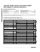
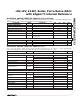
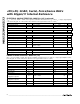
ABSOLUTE MAXIMUM RATINGS
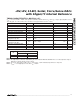
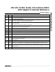
ELECTRICAL CHARACTERISTICS—MAX5132 (+5V)
(V
DD
= +5V ±10%, AGND = DGND, 33nF capacitor at REFADJ, internal reference, R
L
= 5kΩ, C
L
= 100pF, output amplifier connect-
ed in unity-gain, T
A
= T
MIN
to T
MAX
, unless otherwise noted. Typical values are at T
A
= +25°C.)
Stresses beyond those listed under “Absolute Maximum Ratings” may cause permanent damage to the device. These are stress ratings only, and functional
operation of the device at these or any other conditions beyond those indicated in the operational sections of the specifications is not implied. Exposure to
absolute maximum rating conditions for extended periods may affect device reliability.
V
DD
to AGND, DGND...............................................-0.3V to +6V
AGND to DGND.....................................................-0.3V to +0.3V
Digital Inputs to DGND.............................................-0.3V to +6V
Digital Outputs (DOUT, UPO) to DGND.....-0.3V to (V
DD
+ 0.3V)
FB, OUT to AGND ......................................-0.3V to (V
DD
+ 0.3V)
REF, REFADJ to AGND..............................-0.3V to (V
DD
+ 0.3V)
Maximum Current into Any Pin............................................50mA
Continuous Power Dissipation (T
A
= +70°C)
16-Pin QSOP (derate 8.00mW/°C above +70°C)..........667mW
Operating Temperature Range ..........................-40°C to +85°C
Storage Temperature Range.............................-65°C to +150°C
Lead Temperature (soldering, 10sec).............................+300°C
V
IN
= 0 or V
DD
MAX5132A
REFADJ = V
DD
4.5V ≤ V
DD
≤ 5.5V
MAX5132B
MAX5132B
MAX5132A
MAX5132A
T
A
= +25°C
CONDITIONS
pF8C
IN
Input Capacitance
µA-1 0.001 1I
IN
Input Leakage Current
mV200V
HYS
Input Hysteresis
V0.8V
IL
Input Low Voltage
V3V
IH
Input High Voltage
µA3.3 7REFADJ Current
ppm/°C
10
TCV
REF
3
Output Voltage Temperature
Coefficient
V2.475 2.5 2.525V
REF
Output Voltage
-0.5 0.5
Bits13NResolution
µV/V20 250PSRRPower-Supply Rejection Ratio
ppm/°C
10 30
TCV
FS
310
Full-Scale Temperature
Coefficient (Note 3)
LSB-1 1DNLDifferential Nonlinearity
mV-10 10V
OS
Offset Error (Note 2)
-3 -0.2 3 mVGEGain Error
UNITSMIN TYP MAXSYMBOLPARAMETER
I
SINK
= 2mA
I
SOURCE
= 2mA
V0.13 0.4V
OL
Output Low Voltage
VV
DD
- 0.5V
OH
Output High Voltage
MAX5132B
LSB
-1 1
INLIntegral Nonlinearity (Note 1)
0 ≤ I
OUT
≤ 100µA (sourcing) µV/µA50V
OUT
/I
OUT
Reference External Load Regulation
mA4Reference Short-Circuit Current
STATIC PERFORMANCE
REFERENCE
DIGITAL INPUT
DIGITAL OUTPUTS