
Owner manual


MAX5132/MAX5133
+5V/+3V, 13-Bit, Serial, Force/Sense DACs
with 10ppm/°C Internal Reference
_______________________________________________________________________________________ 9
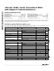
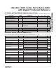
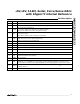
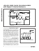
Pin Description
NAME FUNCTION
1 FB Amplifier Inverting Sense Input (Analog Input)
PIN
2 OUT Analog Output Voltage. High impedance if part is in shutdown.
3 RSTVAL
Reset Value Input (Digital Input)
1: Connect to VDD to select midscale as the output reset value.
0: Connect to DGND to select 0V as the output reset value.
4
PDL
Power-Down Lockout (Digital Input).
1: Normal operation.
0: Disallows shutdown (device cannot be powered down).
5
CLR
Reset DAC Input (Digital Input). Clears the DAC to its predetermined (RSTVAL) output state. Clearing the
DAC will cause it to exit a software shutdown state.
6
CS
Active-Low Chip-Select Input (Digital Input)
7 DIN Serial Data Input. Data is clocked in on the rising edge of SCLK.
8 SCLK Serial Clock Input
9 DGND Digital Ground
10 DOUT Serial Data Output
11 UPO User-Programmable Output (Digital Output)
12 PD
Power-Down Input (Digital Input). Pulling PD high when PDL = V
DD
places the IC into shutdown with a
maximum shutdown current of 20µA.
13 AGND Analog Ground
14 REF
Buffered Reference Output/Input. In internal reference mode, the reference buffer provides a +2.5V
(MAX5132) or +1.25V (MAX5133) nominal output, externally adjustable at REFADJ. In external reference
mode, disable the internal reference by pulling REFADJ to V
DD
and applying the external reference to REF.
15 REFADJ
Analog Reference Adjust Input. Bypass with a 33nF capacitor to AGND. Connect to V
DD
when using an
external reference.
16 V
DD
Positive Power Supply. Bypass with a 0.1µF capacitor in parallel with a 4.7µF capacitor to AGND.