
Instruction Manual
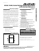

MAX5230/MAX5231
3V/5V, 12-Bit, Serial Voltage-Output Dual DACs
with Internal Reference
10 ______________________________________________________________________________________
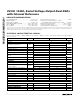
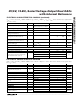
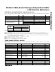
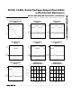
PIN NAME FUNCTION
1 OSA DAC A Offset Adjust
2 OUTA DAC A Output
3 RSTV
Reset Value Input
1: Connect to V
DD
to select midscale as the reset value.
0: Connect to DGND to select zero as the reset value.
4 LDAC Load DACs A and B
5 CLR
Clear Input. Both DAC outputs go to zero or midscale. Clears both DAC internal registers (input
register and DAC register) to its predetermined (RSTV) state.
6 CS Chip-Select Input
7 DIN Serial Data Input. Data is clocked in on the rising edge of SCLK.
8 SCLK Serial Clock Input
9 DGND Digital Ground
10 DOUT Serial Data Output
11 PDL Power-Down Lockout. Disables shutdown of both DACs when low.
12 REF Reference Output. Reference provides a 2.465V (MAX5231) or 1.234V (MAX5230) nominal output.
13 AGND Analog Ground
14 V
DD
Positive Power Supply. Bypass V
DD
with a 0.1µF capacitor in parallel with a 4.7µF capacitor to
AGND, and bypass V
DD
with a 0.1µF capacitor to DGND.
15 OUTB DAC B Output
16 OSB DAC B Offset Adjust
Pin Description
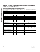
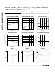
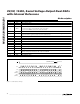
CS
SCLK
DIN
COMMAND EXECUTED
9
8
16 (1)
1
C1
C2 S0
C0
D11
D10
D9
D8 D5 D4 D3 D2 D1
(MODE 0)
(MODE 1)
DOUT
DOUT
C2 C1
C2 C1
D0D7 D6
Figure 1. Serial Interface Timing