
Instruction Manual


MAX5230/MAX5231
Serial Interface
The 3-wire serial interface (SPI, QSPI, MICROWIRE
compatible) used in the MAX5230/MAX5231 allows for
complete control of DAC operations (Figures 4 and 5).
Figures 1 and 2 show the timing for the serial interface.
The serial word consists of 3 control bits followed by 12
data bits (MSB first) and 1 sub-bit as described in
Tables 1, 2, and 3. When the 3 control bits are all zero
or all 1, D11–D8 are used as additional control bits,
allowing for greater DAC functionality.
The digital inputs allow any of the following: loading the
input register(s) without updating the DAC register(s),
updating the DAC register(s) from the input register(s),
or updating the input and DAC register(s) simultane-
ously. The control bits and D11–D8 allow the DACs to
operate independently.
Send the 16-bit data as one 16-bit word (QSPI) or two
8-bit packets (SPI, MICROWIRE), with CS low during
this period. The control bits and D11–D8 determine
which registers update and the state of the registers
when exiting shutdown. The 3-bit control and D11–D8
determine the following:
• Registers to be updated
• Selection of the power-down and shutdown modes
The general timing diagram of Figure 1 illustrates data
acquisition. Driving CS low enables the device to
receive data. Otherwise the interface control circuitry is
disabled. With CS low, data at DIN is clocked into the
register on the rising edge of SCLK. As CS goes high,
data is latched into the input and/or DAC registers,
depending on the control bits and D11–D8. The maxi-
mum clock frequency guaranteed for proper operation
is 13.5MHz. Figure 2 depicts a more detailed timing
diagram of the serial interface.
3V/5V, 12-Bit, Serial Voltage-Output Dual DACs
with Internal Reference
12 ______________________________________________________________________________________
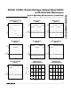
Table 1. Serial Data Format
MSB <------------16-bits of serial data ------------> LSB
3 Control Bits MSB .. 12 Data Bits... LSB Sub-Bit
C2…C0 D11 ..............................D0 S0
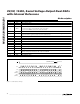
Table 2. Serial-Interface Programming Commands
16-BIT SERIAL WORD
C2 C1 C0 D11..............D0 S0*
FUNCTION
0 0 1 12-bit DAC data 0 Load input register A; DAC registers are unchanged.
0 1 0 12-bit DAC data 0 Load input register A; all DAC registers are updated.
0 1 1 12-bit DAC data 0
Load all DAC registers from the shift register (start up both DACs
with new data, and load the input registers).
1 0 0 X X X X X X X X X X X X 0
Update both DAC registers from their respective input registers (start
up both DACs with data previously stored in the input registers).
1 0 1 12-bit DAC data 0 Load input register B; DAC registers are unchanged.
1 1 0 12-bit DAC data 0 Load input register B; all DAC registers are updated.
1 1 1 P1A P1B X X X X X X X X X X 0
Shut down both DACs, respectively, according to bits P1A and P1B
(see Table 3). Internal bias and reference remain active.
0 0 0 0 0 1 X X X X X X X X X 0
Update DAC register A from input register A (start up DAC A with
data previously stored in input register A).
0 0 0 0 1 1 P1A P1B X X X X X X X 0
Full Power-Down. Power down the main bias generator and shut
down both DACs, respectively, according to bits P1A and P1B (see
Table 3).
0 0 0 1 0 1 X X X X X X X X X 0
Update DAC register B from input register B (start up DAC B with
data previously stored in input register B).
0 0 0 1 1 0 P1A X X X X X X X X 0 Shut down DAC A according to bit P1A (see Table 3).
0 0 0 1 1 1 P1B X X X X X X X X 0 Shut down DAC B according to bit P1B (see Table 3).
0 0 0 1 0 0 0 X X X X X X X X 0 Mode 0. DOUT clocked out on SCLK falling edge (default).
0 0 0 1 0 0 1 X X X X X X X X 0 Mode 1. DOUT clocked out on SCLK rising edge.
X = Don’t care.
* S0 must be zero for proper operation.