
Instruction Manual


MAX5230/MAX5231
Power-Supply and Bypassing
Considerations
On power-up, the input and DAC registers are cleared
to either zero (RSTV = DGND) or midscale (RSTV =
V
DD
). Bypass V
DD
with a 4.7µF capacitor in parallel
with a 0.1µF capacitor to AGND, and bypass V
DD
with
a 0.1µF capacitor to DGND. Minimize lead lengths to
reduce lead inductance.
Grounding and Layout Considerations
Digital and AC transient signals on AGND or DGND can
create noise at the output. Connect AGND and DGND
to the highest quality ground available. Use proper
grounding techniques, such as a multilayer board with a
low-inductance ground plane or star connect all ground
return paths back to the MAX5230/MAX5231 AGND.
Carefully lay out the traces between channels to reduce
AC cross-coupling and crosstalk. Wire-wrapped boards
and sockets are not recommended. If noise becomes
an issue, shielding may be required.
Chip Information
TRANSISTOR COUNT: 4745
PROCESS: BiCMOS
3V/5V, 12-Bit, Serial Voltage-Output Dual DACs
with Internal Reference
16 ______________________________________________________________________________________
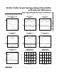
TO OTHER
SERIAL DEVICES
MAX5230
MAX5231
DIN
SCLK
CS
MAX5230
MAX5231
DIN
SCLK
CS
MAX5230
MAX5231
DIN
SCLK
CS
DIN
SCLK
CS1
CS2
CS3
Figure 9. Multiple MAX5230/MAX5231s Sharing a Common DIN Line
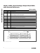
TO OTHER
SERIAL DEVICES
MAX5230
MAX5231
DIN
SCLK
CS
MAX5230
MAX5231
MAX5230
MAX5231
DIN
DOUT DOUT DOUT
SCLK
CS
DIN
SCLK
CS
CS
SCLK
DIN
Figure 10. Daisy-Chaining MAX5230/MAX5231 Devices