
Instruction Manual
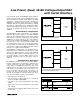

__________________General Description
The +5V MAX5250 combines four low-power, voltage-
output, 10-bit digital-to-analog converters (DACs) and
four precision output amplifiers in a space-saving, 20-
pin package. In addition to the four voltage outputs,
each amplifier’s negative input is also available to the
user. This facilitates specific gain configurations, remote
sensing, and high output drive capacity, making the
MAX5250 ideal for industrial-process-control applica-
tions. Other features include software shutdown, hard-
ware shutdown lockout, an active-low reset that clears
all registers and DACs to zero, a user-programmable
logic output, and a serial-data output.
Each DAC has a double-buffered input organized as an
input register followed by a DAC register. A 16-bit serial
word loads data into each input/DAC register. The
3-wire serial interface is compatible with SPI™/QSPI™
and Microwire™. It allows the input and DAC registers to
be updated independently or simultaneously with a sin-
gle software command. All logic inputs are TTL/CMOS-
logic compatible.
________________________Applications
Digital Offset and Gain Adjustment
Microprocessor-Controlled Systems
Industrial Process Controls
Automatic Test Equipment
Remote Industrial Controls
Motion Control
______________________________Features
♦ Four 10-Bit DACs with Configurable
Output Amplifiers
♦ +5V Single-Supply Operation
♦ Low Supply Current: 0.85mA Normal Operation
10µA Shutdown Mode
♦ Available in 20-Pin SSOP and DIP Packages
♦ Power-On Reset Clears all Registers and
DACs to Zero
♦ SPI/QSPI and Microwire Compatible
♦ Simultaneous or Independent Control of DACs
via 3-Wire Serial Interface
♦ User-Programmable Digital Output
♦ Schmitt-Trigger Inputs for Direct Optocoupler
Interface
♦ 12-Bit Upgrade Available: MAX525
MAX5250
Low-Power, Quad, 10-Bit Voltage-Output DAC
with Serial Interface
________________________________________________________________
Maxim Integrated Products
1
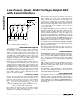
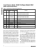
MAX5250
OUTA
FBA
FBB
FBC
FBD
DAC A
DAC B
DAC C
DAC D
REFAB
DAC
REGISTER A
DECODE
CONTROL
INPUT
REGISTER A
DAC
REGISTER B
INPUT
REGISTER B
DAC
REGISTER C
INPUT
REGISTER C
DAC
REGISTER D
INPUT
REGISTER D
16-BIT
SHIFT
REGISTER
SR
CONTROL
LOGIC
OUTPUT
CS
DIN
SCLK
OUTB
OUTC
OUTD
DOUT
PDL
CL
V
DD
AGND
DGND
UPO REFCD
_________________________________________________________________________Functional Diagram
19-1171; Rev 0; 12/96
_________________Ordering Information
Ordering Information continued on last page.
Pin Configuration appears at end of data sheet.
For free samples & the latest literature: http://www.maxim-ic.com, or phone 1-800-998-8800
SPI and QSPI are trademarks of Motorola, Inc. Microwire is a trademark of National Semiconductor Corp.
PART
MAX5250ACPP
MAX5250BCPP
MAX5250ACAP 0°C to +70°C
0°C to +70°C
0°C to +70°C
TEMP. RANGE PIN-PACKAGE
20 Plastic DIP
20 Plastic DIP
20 SSOP
INL
(LSB)
±1/2
±1
±1/2
MAX5250BCAP 0°C to +70°C 20 SSOP ±1