
Instruction Manual


Power-Down (PDL)
The power-down lockout pin PDL disables software
shutdown when low. When in shutdown, transitioning
PDL from high to low wakes up the part with the output
set to the state prior to shutdown. PDL can also be
used to wake up the device asynchronously.
Daisy Chaining Devices
Any number of MAX5250s can be daisy chained by
connecting the DOUT pin of one device to the DIN pin
of the following device in the chain (Figure 7).
Since the MAX5250’s DOUT pin has an internal active
pull-up, the DOUT sink/source capability determines
the time required to discharge/charge a capacitive
load. Refer to the serial-data-out V
OH
and V
OL
specifi-
cations in the
Electrical Characteristics.
Figure 8 shows an alternate method of connecting sev-
eral MAX5250s. In this configuration, the data bus is
common to all devices; data is not shifted through a
daisy chain. More I/O lines are required in this configu-
ration because a dedicated chip-select input (CS) is
required for each IC.
MAX5250
Low-Power, Quad, 10-Bit Voltage-Output DAC
with Serial Interface
______________________________________________________________________________________ 11
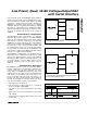
CS
SCLK
DIN
DOUT
(MODE 1)
MSB FROM
PREVIOUS WRITE
MSB FROM
PREVIOUS WRITE
COMMAND
EXECUTED
9
8
16
1
A0
A1 S0
C1
C0
D9
D8
D7
D4
D3
D2
D1
D0
S1
D6
D5
DOUT
(MODE 0)
A0
A1 S0 A1
C1
C0
D9
D8
D7
D4
D3
D2
D1
D0
S1
D6
D5
A0
A1 S0 A1
C1
C0
D9
D8
D7
D4
D3
D2
D1
D0
S1
D6
D5
DATA PACKET (N)
DATA PACKET (N-1)
DATA PACKET (N)
DATA PACKET (N-1)
DATA PACKET (N)
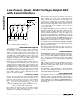
Figure 5. Serial-Interface Timing Diagram
SCLK
DIN
DOUT
t
CSO
t
CSS
t
CL
t
CH
t
CP
t
DO1
t
CSW
t
CS1
t
DO2
t
CSH
t
DS
t
DH
CS
Figure 6. Detailed Serial-Interface Timing Diagram