
Instruction Manual


MAX5250
Using an AC Reference
In applications where the reference has AC signal com-
ponents, the MAX5250 has multiplying capability within
the reference input range specifications. Figure 12
shows a technique for applying a sine-wave signal to
the reference input where the AC signal is offset before
being applied to REFAB/REFCD. The reference voltage
must never be more negative than DGND.
The MAX5250’s total harmonic distortion plus noise
(THD + N) is typically less than -72dB (full-scale code),
given a 1Vp-p signal swing and input frequencies up to
25kHz. The typical -3dB frequency is 650kHz, as
shown in the
Typical Operating Characteristics
graphs.
Digitally Programmable Current Source
The circuit of Figure 13 places an NPN transistor
(2N3904 or similar) within the op-amp feedback loop to
implement a digitally programmable, unidirectional cur-
rent source. This circuit can be used to drive 4–20mA
current loops, which are commonly used in industrial-
control applications. The output current is calculated
with the following equation:
I
OUT
= (V
REF
/ R) x (NB / 1024)
where NB is the numeric value of the DAC’s binary
input code and R is the sense resistor shown in
Figure 13.
Low-Power, Quad, 10-Bit Voltage-Output DAC
with Serial Interface
14 ______________________________________________________________________________________
MAX5250
DAC A
DAC B
DAC C
DAC D
V
REFAB
= V
REFCD
= 2.5V
OUTA
10k
10k
10k
10k
10k
10k
10k
10k
OUTB
OUTC
OUTD
DGNDAGND
REFAB
REFCD
REFERENCE INPUTS
+5V
V
DD
FBA
FBB
FBC
FBD
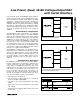
Figure 10. Unipolar Rail-to-Rail Output Circuit
DAC
V
OUT
+5V
-5V
R1 = R2 = 10kΩ ± 0.1%
MAX5250
REF_
R1
R2
FB_
OUT_
Figure 11. Bipolar Output Circuit
DAC_
OUT_
MAX5250
10k
26k
REF_
V
DD
AGND DGND
+5V
AC
REFERENCE
INPUT
500mVp-p
1/2 MAX492
Figure 12. AC Reference Input Circuit