
Instruction Manual


Power-Supply Considerations
On power-up, all input and DAC registers are cleared
(set to zero code) and DOUT is in Mode 0 (serial data
is shifted out of DOUT on the clock’s falling edge).
For rated MAX5250 performance, limit REFAB/REFCD
to less than 1.4V below V
DD
. Bypass V
DD
with a 4.7µF
capacitor in parallel with a 0.1µF capacitor to AGND.
Use short lead lengths and place the bypass capaci-
tors as close to the supply pins as possible.
Grounding and Layout Considerations
Digital or AC transient signals between AGND and
DGND can create noise at the analog outputs. Tie
AGND and DGND together at the DAC, then tie this
point to the highest-quality ground available.
Good printed circuit board ground layout minimizes
crosstalk between DAC outputs, reference inputs, and
digital inputs. Reduce crosstalk by keeping analog
lines away from digital lines. Wire-wrapped boards are
not recommended.
MAX5250
Low-Power, Quad, 10-Bit Voltage-Output DAC
with Serial Interface
______________________________________________________________________________________ 15
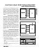
DAC_
MAX5250
REF_
OUT_
R
I
OUT
2N3904
V
L
FB_
Figure 13. Digitally Programmable Current Source
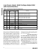
__________________Pin Configuration
20
19
18
17
16
15
14
13
1
2
3
4
5
6
7
8
V
DD
FBD
OUTD
OUTCOUTB
OUTA
FBA
AGND
TOP VIEW
FBC
REFCD
PDL
UPOCS
CL
REFAB
FBB
12
11
9
10
DOUT
DGNDSCLK
DIN
DIP/SSOP
MAX5250