
Instruction Manual

MAX5250
Low-Power, Quad, 10-Bit Voltage-Output DAC
with Serial Interface
_______________________________________________________________________________________ 3
ELECTRICAL CHARACTERISTICS (continued)
(V
DD
= +5V ±10%, AGND = DGND = 0V, REFAB = REFCD = 2.5V, R
L
= 5kΩ, C
L
= 100pF, T
A
= T
MIN
to T
MAX
, unless otherwise
noted. Typical values are at T
A
= +25°C. Output buffer connected in unity-gain configuration (Figure 9).)
Note 1: Guaranteed from code 3 to code 1023 in unity-gain configuration.
Note 2: Accuracy is better than 1LSB for V
OUT
= 6mV to V
DD
- 60mV, guaranteed by a power-supply rejection test at the
end points.
Note 3: R
L
= ∞, digital inputs at DGND or V
DD
.
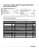
PARAMETER SYMBOL MIN TYP MAX UNITS
Output High Voltage V
OH
V
DD
- 0.5 V
Input Capacitance C
IN
8 pF
Input Leakage Current I
IN
0.01 ±1.0 µA
Reference Current in Shutdown 0.01 ±1 µA
Output Low Voltage V
OL
0.13 0.4 V
Voltage Output Slew Rate SR 0.6 V/µs
Input High Voltage V
IH
2.4 V
Input Low Voltage V
IL
0.8 V
Output Settling Time 10 µs
Output Voltage Swing 0 to V
DD
V
Current into FB_ 0 0.1 µA
OUT_ Leakage Current
in Shutdown
0.01 ±1 µA
Start-Up Time Exiting
Shutdown Mode
15 µs
Digital Feedthrough 5 nV-s
Digital Crosstalk 5 nV-s
Supply Voltage V
DD
4.5 5.5 V
Supply Current I
DD
0.85 0.98 mA
Supply Current in Shutdown 10 20 µA
CONDITIONS
To ±1/2LSB, V
STEP
= 2.5V
I
SOURCE
= 2mA
Rail-to-rail (Note 2)
V
IN
= 0V or V
DD
I
SINK
= 2mA
R
L
= ∞
CS = V
DD
, DIN = 100kHz
(Note 3)
(Note 3)
DIGITAL INPUTS
DIGITAL OUTPUTS
DYNAMIC PERFORMANCE
POWER SUPPLIES