
Manual

MAX5383/MAX5384/MAX5385
Low-Cost, Low-Power, 8-Bit DACs with 3-Wire
Serial Interface in SOT23
2 _______________________________________________________________________________________
ABSOLUTE MAXIMUM RATINGS
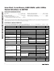
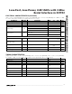
ELECTRICAL CHARACTERISTICS
(V
DD
= +2.7V to +3.6V (MAX5383), V
DD
= +4.5V to +5.5V (MAX5384), V
DD
= +2.7V to +5.5V (MAX5385), R
L
= 10kΩ, C
L
= 50pF,
T
A
= T
MIN
to T
MAX
, unless otherwise noted. Typical values are T
A
= +25°C.)
Stresses beyond those listed under “Absolute Maximum Ratings” may cause permanent damage to the device. These are stress ratings only, and functional
operation of the device at these or any other conditions beyond those indicated in the operational sections of the specifications is not implied. Exposure to
absolute maximum rating conditions for extended periods may affect device reliability.
V
DD
to GND..............................................................-0.3V to +6V
OUT ............................................................-0.3V to (V
DD
+ 0.3V)
CS, SCLK, DIN to GND ............................................-0.3V to +6V
Maximum Current into Any Pin............................................50mA
Continuous Power Dissipation (T
A
= +70°C)
6-Pin SOT23 (derate 8.7mW/°C above +70°C)..........696mW
Operating Temperature Range ...........................-40°C to +85°C
Storage Temperature Range .............................-65°C to +150°C
Maximum Junction Temperature .....................................+150°C
Lead Temperature (soldering, 10s) .................................+300°C
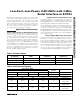
PARAMETER SYMBOL CONDITIONS MIN TYP MAX UNITS
STATIC ACCURACY
Resolution 8 Bits
Integral Linearity Error INL (Note 1) ±1 LSB
Differential Linearity Error DNL Guaranteed monotonic ±1 LSB
Offset Error V
OS
(Note 2) ±1 ±25 mV
Offset Error Supply Rejection MAX5385 (Notes 2, 3) 60 dB
MAX5383/MAX5384 3
Offset Error Temperature
Coefficient
MAX5385 1
ppm/ °C
M AX 5383/M AX 5384 10
Full-Scale Error C ode = 255, no l oad
MAX5385 5
% of
i d eal FS
Full-Scale Error Supply
Rejection
C od e = 255 ( N ote 4) M AX 5383/M AX 5384 50 dB
M AX 5383/M AX 5384 ±40
Full-Scale Error Temperature
Coefficient
Code = 255
MAX5385 ±10
ppm/ °C
DAC OUTPUT
MAX5383 1.8 2 2.2
MAX5384 3.6 4 4.4
Internal Reference Voltage
(Note 5)
REF
MAX5385
0.85 ×
V
DD
0.9 ×
V
DD
0.95 ×
V
DD
V
Code = 255, 0µA to 100µA0.5
Output Load Regulation
Code = 0, 0µA to 100µA0.5
LSB
[D13, D12] = 0, 1 1k
[D13, D12] = 1, 0 100k
Shutdown Output Resistance
to GND
V
OUT
= 0 to V
DD
[D13, D12] = 1, 1 1M
Ω
DYNAMIC PERFORMANCE
Voltage Output Slew Rate Positive and negative 0.4 V/µs
Output Settling Time To 1/2 LSB, 50kΩ and 50pF load (Note 6) 20 µs
Digital Feedthrough Code = 0, all digital inputs from 0 to V
DD
2 nVs