
Manual
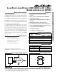

Detailed Description
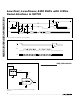
The MAX5383/MAX5384/MAX5385 voltage-output, 8-bit
DACs ensure monotonic performance by offering full 8-
bit performance with less than 1LSB integral nonlineari-
ty error and less than 1LSB differential nonlinearity
error. The devices use a simple 3-wire, SPI/QSPI/
MICROWIRE-compatible serial interface that operates
up to 10MHz. They include an internal reference, an
output buffer, and three low-current shutdown modes,
making these devices ideal for low-power, highly inte-
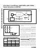
grated applications. Figure 1 shows the devices’ func-
tional diagram.
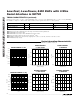
Analog Section
The MAX5383/MAX5384/MAX5385 employ a current-
steering DAC topology as shown in Figure 2. At the
core of the DAC is a reference voltage-to-current con-
verter (V/I) that generates a reference current. This cur-
rent is mirrored to 255 equally weighted current
sources. DAC switches control the outputs of these cur-
rent mirrors so that only the desired fraction of the total
current-mirror currents is steered to the DAC output.
The current is then converted to a voltage across a
resistor, and this voltage is buffered by the output
buffer amplifier.
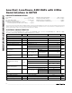
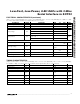
Output Voltage
Table 1 shows the relationship between the DAC code
and the analog output voltage. The 8-bit DAC code is
binary unipolar with 1LSB = (V
REF
/256). The MAX5383/
MAX5384 have a full-scale output voltage of (+2V - 1LSB)
and (+4V - 1LSB), set by the internal references. The
MAX5385 has a full-scale output voltage of (0.9
✕
V
DD
-
1LSB).
Output Buffer
The DAC voltage output is an internally buffered unity-
gain follower that slews up to ±0.4V/µs. The output can
swing from 0 to full scale. With a 1/4FS to 3/4FS output
transition, the amplifier outputs typically settle to
1/2LSB in less than 5µs when loaded with 10kΩ in par-
allel with 50pF. The buffer amplifiers are stable with any
MAX5383/MAX5384/MAX5385
Low-Cost, Low-Power, 8-Bit DACs with 3-Wire
Serial Interface in SOT23
_______________________________________________________________________________________ 7
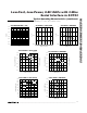
Typical Operating Characteristics (continued)
(V
DD
= +3.0V (MAX5383), V
DD
= +5.0V (MAX5384/MAX5385), T
A
= +25°C, unless otherwise noted.)
2µs/div
MAX5383
OUTPUT SETTLING
1LSB STEP UP
MAX5383/4/5-22
OUT
20mV/div
AC-COUPLED
0 x 7F TO 0 x 80
CS
3V/div
MAX5383
OUTPUT SETTLING
1LSB STEP DOWN
MAX5383/4/5-23
OUT
20mV/div
AC-COUPLED
2µs/div
0 x 80 TO 0 x 7F
CS
3V/div
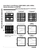
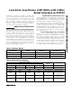
Pin Description
PIN NAME DESCRIPTION
1 OUT DAC Voltage Output
2 GND Ground
3V
DD
Power-Supply Input
4 DIN Serial Data Input
5 SCLK Serial Clock Input
6 CS Chip-Select Input