
Manual

combination of resistive loads >10kΩ and capacitive
loads <50pF.
Power-On Reset
The MAX5383/MAX5384/MAX5385 have a power-on
reset circuit to set the DAC’s output to 0 when V
DD
is
first applied or when V
DD
dips below 1.7V (typ). This
ensures that unwanted DAC output voltages will not
occur immediately following a system startup, such as
after a loss of power. The output glitch on startup is typ-
ically less than 50mV.
Shutdown Mode
The MAX5383/MAX5384/MAX5385 include three soft-
ware-controlled shutdown modes that reduce the supply
current to <1µA. All internal circuitry is disabled, and a
known impedance is placed from OUT to GND to
ensure 0V while in shutdown. Table 2 details the three
shutdown modes of operation.
Digital Section
3-Wire Serial Interface
The MAX5383/MAX5384/MAX5385s’ digital interface is
a standard 3-wire connection compatible with
SPI/QSPI/MICROWIRE interfaces. The chip-select input
(CS) frames the serial data loading at the data-input pin
(DIN). Immediately following CS’s high-to-low transition,
the data is shifted synchronously and latched into the
input register on the rising edge of the serial clock input
(SCLK). After 16 bits have been loaded into the serial
MAX5383/MAX5384/MAX5385
Low-Cost, Low-Power, 8-Bit DACs with 3-Wire
Serial Interface in SOT23
8 _______________________________________________________________________________________
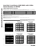
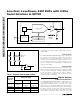
REF
CONTROL LOGIC
DATA LATCH
GND
OUT
V
DD
CURRENT-STEERING
DAC
SERIAL INPUT REGISTERSCLK
DIN
CS
255
8
MAX5383
MAX5384
MAX5385
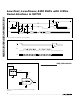
Figure 1. Functional Diagram
SW1 SW2 SW255
OUT
V
REF
Figure 2. Current-Steering DAC Topology
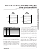
OUTPUT VOLTAGE
DAC CODE
[D11–D4]
MAX5383 MAX5384 MAX5385
1111 1111
2V
×
(255/256)
4V
×
(255/256)
0.9
× V
DD
×
(255/256)
1000 0000 1V 2V 0.9 × V
DD
/ 2
0000 0001 7.8mV 15.6mV 0.9 × V
DD
/ 256
0000 0000 0 0 0
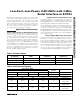
Table 1. Unipolar Code Output Voltage