
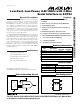
Manual

input register, it transfers its contents to the DAC latch
on CS’s low-to-high transition (Figure 3). Note that if CS
is not kept low during the entire 16 SCLK cycles, data
will be corrupted. In this case, reload the DAC latch
with a new 16-bit word. The serial clock (SCLK) can
idle either high or low between transitions. Figure 4
shows the complete 3-wire serial interface transmis-
sion. Table 3 lists serial interface mapping.
Applications Information
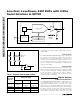
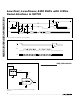
Device Powered by an External Reference
Since the MAX5385 generates an output voltage pro-
portional to V
DD
, a noisy power supply will affect the
accuracy of the on-board reference, thereby affecting
the overall accuracy of the DAC. The circuit in Figure 5
rejects this power-supply noise by powering the device
directly with a precision voltage reference, improving
overall system accuracy. The MAX6103 (+3V, 75ppm)
or the MAX6105 (+5V, 75ppm) precision voltage refer-
ences are ideal choices due to the low power require-
ments of the MAX5385. This solution is also useful
when the required full-scale output voltage is different
from the available supply voltages.
Digital Inputs and Interface Logic
The digital interface for the 8-bit DAC is based on a
3-wire standard that is compatible with SPI, QSPI, and
MICROWIRE interfaces. The three digital inputs (CS, DIN,
and SCLK) load the digital input serially into the DAC.
All the digital inputs include Schmitt-trigger buffers to
accept slow-transition interfaces. This means that opto-
couplers can interface directly to the MAX5383/
MAX5384/MAX5385 without additional external logic.
The digital inputs are compatible with CMOS logic levels
and can be driven with voltages up to +5.5V regardless
of the supply voltage.
Power-Supply Bypassing and Layout
Careful PC board layout is important for best system
performance. To reduce crosstalk and noise injection,
keep analog and digital signals separate. To ensure
that the ground return from GND to the supply ground
is short and low impedance, a ground plane is recom-
mended. Bypass V
DD
with a 0.1µF capacitor to ground
as close as possible to the device. If the supply is
excessively noisy, connect a 10Ω resistor in series with
the supply and V
DD
and add additional capacitance.
MAX5383/MAX5384/MAX5385
Low-Cost, Low-Power, 8-Bit DACs with 3-Wire
Serial Interface in SOT23
_______________________________________________________________________________________ 9
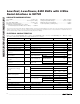
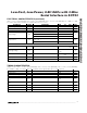
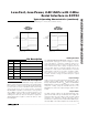
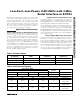
Table 3. Serial Interface Mapping
X = Don’t care
16-BIT SERIAL WORD
ANALOG
MSB LSB OUTPUT
FUNCTION
XX00 0000 0000 XXXX 0V Normal operation
XX00 1111 1111 XXXX
V
REF
× (255/256)
Normal operation
XX00 0000 0001 XXXX V
REF
× (1/256) Normal operation
XX00 1000 0000 XXXX V
REF
× (128/256) Normal operation
XX01 XXXX XXXX XXXX 0V
Shutdown,
1kΩ to GND
XX10 XXXX XXXX XXXX 0V
Shutdown,
100kΩ to GND
XX11 XXXX XXXX XXXX 0V
Shutdown,
1MΩ to GND
Table 2. Shutdown Modes
DAC CODE
[D13 AND D12]
MODE
OUTPUT RESISTANCE TO
GROUND (Ω)
MAXIMUM SUPPLY
CURRENT (µA)
01 Shutdown 1k 1
10 Shutdown 100k 1
11 Shutdown 1M 1