
Manual


MAX5477/MAX5478/MAX5479
Dual, 256-Tap, Nonvolatile, I
2
C-Interface,
Digital Potentiometers
8 _______________________________________________________________________________________
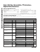
Pin Description
PIN
TSSOP
THIN QFN
NAME
FUNCTION
1 15 HA Potentiometer A High Terminal
2 14 WA Potentiometer A Wiper Terminal
3 13 LA Potentiometer A Low Terminal
4 12 HB Potentiometer B High Terminal
5 11 WB Potentiometer B Wiper Terminal
6 10 LB Potentiometer B Low Terminal
79WP
Write-Protect Input. Connect to GND to allow changes to the wiper position and the data stored
in the EEPROM. Connect to V
DD
or leave open to enable the write protection of the EEPROM.
87
GND
Ground
9 6 A2 Address Input 2. Connect to V
DD
or GND (see Table 1).
10 5 A1 Address Input 1. Connect to V
DD
or GND (see Table 1).
11 4 A0 Address Input 0. Connect to V
DD
or GND (see Table 1).
12 3
SDA
I
2
C Serial Data
13 2
SCL
I
2
C Clock Input
14 1
V
DD
Power-Supply Input. Connect a +2.7V to +5.25V power supply to V
DD
and bypass V
DD
to GND
with a 0.1µF capacitor installed as close to the device as possible.
— 8, 16
N.C.
No Connection. Do not connect.
— EP EP Exposed Paddle. Do not connect.
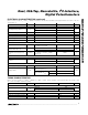
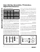
SDA
SCL
START
CONDITION
(S)
t
HD:STA
t
R
t
F
t
HIGH
t
LOW
t
SU:DAT
t
HD:DAT
REPEATED START
CONDITION
(SR)
t
HD:STA
t
SU:STA
t
SU:STO
t
BUF
STOP
CONDITION
(P)
START
CONDITION
(S)
ACKNOWLEDGE
(A)
PARAMETERS ARE MEASURED FROM 30% TO 70%.
Detailed Description
The MAX5477/MAX5478/MAX5479 contain two resistor
arrays with 255 elements in each array. The MAX5477
has a total end-to-end resistance of 10kΩ, the
MAX5478 has an end-to-end resistance of 50kΩ, and
the MAX5479 has an end-to-end resistance of 100kΩ.
The MAX5477/MAX5478/MAX5479 provide access to
the high, low, and wiper terminals for a standard volt-
age-divider configuration. Connect H_, L_, and W_ in
any desired configuration as long as their voltages
remain between GND and V
DD
.
Figure 1. I
2
C Serial-Interface Timing Diagram