
Owner manual


MAX5548
Dual, 8-Bit, Programmable, 30mA
High-Output-Current DAC
4 _______________________________________________________________________________________
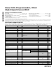
ELECTRICAL CHARACTERISTICS (continued)
(V
DD
= +2.7V to +5.25V, GND = 0, V
REFIN
= +1.25V, internal reference, R
FSADJ_
= 20kΩ; compliance voltage = (V
DD
- 0.6V),
V
SCLK/SCL
= 0, T
A
= -40°C to +85°C, unless otherwise noted. Typical values are at V
DD
= +3.0V and T
A
= +25°C.) (Note 1)
PARAMETER SYMBOL CONDITIONS MIN TYP MAX UNITS
Setup Time for STOP Condition t
SU:STO
160 ns
Maximum Capacitive Load for
Each Bus Line
C
B
400 pF
SPI TIMING CHARACTERISTICS (Figure 6)
SCLK Clock Period t
CP
100 ns
SCLK Pulse-Width High t
CH
40 ns
SCLK Pulse-Width Low t
CL
40 ns
CS Fall to SCLK Rise Setup Time t
CSS
25 ns
SCLK Rise to CS Rise Hold Time t
CSH
50 ns
DIN Setup Time t
DS
40 ns
DIN Hold Time t
DH
0ns
SCLK Fall to DOUT Transition t
DO1
C
LOAD
= 30pF 40 ns
CS Fall to DOUT Enable t
CSE
C
LOAD
= 30pF 40 ns
CS Rise to DOUT Disable t
CSD
C
LOAD
= 30pF 40 ns
SCLK Rise to CS Fall Delay t
CS0
50 ns
CS Rise to SCLK Rise Hold Time t
CS1
40 ns
CS Pulse-Width High t
CSW
100 ns
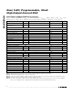
SPI TIMING CHARACTERISTICS FOR DAISY CHAINING (Figure 6)
SCLK Clock Period t
CP
200 ns
SCLK Pulse-Width High t
CH
80 ns
SCLK Pulse-Width Low t
CL
80 ns
CS Fall to SCLK Rise Setup Time t
CSS
25 ns
SCLK Rise to CS Rise Hold Time t
CSH
50 ns
DIN Setup Time t
DS
40 ns
DIN Hold Time t
DH
0ns
SCLK Fall to DOUT Transition t
DO1
C
LOAD
= 30pF 40 ns
CS Fall to DOUT Enable t
CSE
C
LOAD
= 30pF 40 ns
CS Rise to DOUT Disable t
CSD
C
LOAD
= 30pF 40 ns
SCLK Rise to CS Fall Delay t
CS0
50 ns
CS Rise to SCLK Rise Hold Time t
CS1
40 ns
CS Pulse-Width High t
CSW
100 ns
Note 1: 100% production tested at T
A
= +25°C. Limits over temperature are guaranteed by design.
Note 2: INL linearity is guaranteed from code 15 to code 255.
Note 3: Connect a resistor from FSADJ_ to GND to adjust the full-scale current. See the Reference Architecture and Operation section.
Note 4: Settling time is measured from (0.25 x full scale) to (0.75 x full scale).
Note 5: The device draws higher supply current when the digital inputs are driven with voltages between (V
DD
- 0.5V) and (GND +
0.5V). See the Supply Current vs. Digital Input Voltage graph in the Typical Operating Characteristics.