
Manual

MAX5886
3.3V, 12-Bit, 500Msps High Dynamic
Performance DAC with Differential LVDS Inputs
10 ______________________________________________________________________________________
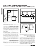
Figure 3 displays a simplified diagram of the
MAX5886’s internal output structure.
Clock Inputs (CLKP, CLKN)
The MAX5886 features a flexible differential clock input
(CLKP, CLKN) operating from separate supplies
(VCLK, CLKGND) to achieve the lowest possible jitter
performance. The two clock inputs can be driven from
a single-ended or a differential clock source. For sin-
gle-ended operation, CLKP should be driven by a logic
source, while CLKN should be bypassed to AGND with
a 0.1µF capacitor.
The CLKP and CLKN pins are internally biased to 1.5V.
This allows the user to AC-couple clock sources directly
to the device without external resistors to define the DC
level. The input resistance of CLKP and CLKN is >5kΩ.
See Figure 4 for a convenient and quick way to apply a
differential signal created from a single-ended source
(e.g., HP 8662A signal generator) and a wideband
transformer. These inputs can also be driven from an
LVDS-compatible clock source; however, it is recom-
mended to use sinewave or AC-coupled ECL drive for
best performance.
Data Timing Relationship
Figure 5 shows the timing relationship between differ-
ential, digital LVDS data, clock, and output signals. The
MAX5886 features a 1.8ns hold, a -0.8ns setup, and a
1.8ns propagation delay time. There is a four-clock-
cycle latency between CLKP/CLKN transitioning
high/low and IOUTP/IOUTN.
LVDS-Compatible Digital Inputs
(B0P–B11P, B0N–B11N)
The MAX5886 features LVDS receivers on the bus input
interface. These LVDS inputs (B0P/N through B11P/N)
allow for a low-differential voltage swing with low con-
stant power consumption across a large range of
frequencies. Their differential characteristic supports
the transmission of high-speed data patterns without
the negative effects of electromagnetic interference
(EMI). All MAX5886 LVDS inputs feature on-chip termi-
nation with differential 100Ω resistors. See Figure 6 for
a simplified block diagram of the LVDS inputs.
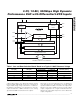
0.1µF
1.2V
REFERENCE
10kΩ
I
REF
R
SET
DACREF
FSADJ
REFIO
I
REF
= V
REFIO
/R
SET
CURRENT-STEERING
DAC
AV
DD
IOUTP
IOUTN
Figure 2. Reference Architecture, Internal Reference
Configuration
I
OUT
I
OUT
IOUTN IOUTP
CURRENT
SOURCES
CURRENT
SWITCHES
AV
DD
Figure 3. Simplified Analog Output Structure
SINGLE-ENDED
CLOCK SOURCE
(e.g., HP 8662A)
1:1
WIDEBAND RF TRANSFORMER
PERFORMS SINGLE-ENDED TO
DIFFERENTIAL CONVERSION.
TO
DAC
CLKP
0.1µF
0.1µF
CLKN
CLKGND
25Ω
25Ω
Figure 4. Differential Clock Signal Generation