
Manual


MAX5886
3.3V, 12-Bit, 500Msps High Dynamic
Performance DAC with Differential LVDS Inputs
______________________________________________________________________________________ 11
A common-mode level of 1.25V and an 800mV differen-
tial input swing can be applied to these inputs.
Segment Shuffling (SEL0)
Segment shuffling can improve the SFDR of the
MAX5886. The improvement is most pronounced at
higher output frequencies and amplitudes. Note that an
improvement in SFDR can only be achieved at the cost
of a slight increase in the DAC’s noise floor.
Pin SEL0 controls the segment-shuffling function. If
SEL0 is pulled low, the segment-shuffling function of
the DAC is disabled. SEL0 can also be left open,
because an internal pulldown resistor helps to deacti-
vate the segment-shuffling feature. To activate the
MAX5886 segment-shuffling function, SEL0 must be
pulled high.
Power-Down Operation (PD)
The MAX5886 also features an active-high power-down
mode, which allows the user to cut the DAC’s current
consumption. A single pin (PD) is used to control the
power-down mode (PD = 1) or reactivate the DAC (PD
= 0) after power-down. Enabling the power-down mode
of the MAX5886 allows the overall power consumption
to be reduced to less than 1mW. The MAX5886
requires 10ms to wake up from power-down and enter
a fully operational state.
Applications Information
Differential Coupling Using a
Wideband RF Transformer
The differential voltage existing between IOUTP and
IOUTN can also be converted to a single-ended volt-
age using a transformer (Figure 7) or a differential
amplifier configuration. Using a differential transformer-
coupled output, in which the output power is limited to
0dBm, can optimize the dynamic performance.
However, make sure to pay close attention to the trans-
former core saturation characteristics when selecting a
transformer for the MAX5886. Transformer core satura-
tion can introduce strong 2nd-harmonic distortion,
especially at low output frequencies and high signal
amplitudes. It is also recommended to center tap the
transformer to ground. If no transformer is used, each
DAC output should be terminated to ground with a 50Ω
resistor. Additionally, a 100Ω resistor should be placed
between the outputs (Figure 8).
B0 TO B11
CLKP
IOUT
N - 1
N
N + 1 N + 2
N - 6 N - 4
N - 2
N - 3
N - 3
t
SETUP
t
HOLD
t
PD
t
CH
t
CL
Figure 5. Detailed Timing Relationship
100Ω
B0P–B11P
B0N–B11N
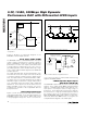
DQ
D
Q
CLOCK
TO DECODE
LOGIC
Figure 6. Simplified LVDS-Compatible Input Structure