
Manual


MAX5886
3.3V, 12-Bit, 500Msps High Dynamic
Performance DAC with Differential LVDS Inputs
______________________________________________________________________________________ 15
supply decoupling guidelines for high-speed, high-fre-
quency applications should be closely followed.
This reduces EMI and internal crosstalk that can signifi-
cantly affect the dynamic performance of the MAX5886.
Use of a multilayer printed circuit (PC) board with sepa-
rate ground and power-supply planes is recommend-
ed. High-speed signals should run on lines directly
above the ground plane. Since the MAX5886 has sepa-
rate analog and digital ground buses (AGND,
CLKGND, and DGND, respectively), the PC board
should also have separate analog and digital ground
sections with only one point connecting the two planes.
Digital signals should be run above the digital ground
plane and analog/clock signals above the analog/clock
ground plane. Digital signals should be kept as far
away from sensitive analog inputs, reference input
sense lines, common-mode input, and clock inputs as
practical. A symmetric design of clock input and ana-
log output lines is recommended to minimize 2nd-order
harmonic distortion components and optimize the
DAC’s dynamic performance. Digital signal paths
should be kept short and run lengths matched to avoid
propagation delay and data skew mismatches.
The MAX5886 supports three separate power-supply
inputs for analog (AV
DD
), digital (DV
DD
), and clock
(VCLK) circuitry. Each AV
DD
, DV
DD
, and VCLK input
should at least be decoupled with a separate 0.1µF
capacitor as close to the pin as possible and their
opposite ends with the shortest possible connection to
the corresponding ground plane (Figure 13). Try to
minimize the analog and digital load capacitances for
optimized operation. All three power-supply voltages
should also be decoupled at the point they enter the
PC board with tantalum or electrolytic capacitors.
Ferrite beads with additional decoupling capacitors
forming a pi network could also improve performance.
The analog and digital power-supply inputs AV
DD
,
VCLK, and DV
DD
of the MAX5886 allow a supply volt-
age range of 3.3V ±5%.
The MAX5886 is packaged in a 68-pin QFN-EP
(package code: G6800-4), providing greater design
flexibility, increased thermal efficiency**, and optimized
AC performance of the DAC. The exposed pad (EP)
enables the user to implement grounding techniques,
which are necessary to ensure highest performance
operation. The EP must be soldered down to AGND.
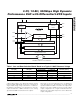
O
-30
-60
-70
-73
-75
-80
-90
0.2 0.4 0.6 1.2 1.8 6.0
IMD REQUIREMENT: < -70dBc
30kHz 100kHz
MEASUREMENT BANDWIDTH
TRANSMITTER EDGE
INBAND OUTBAND
WORST-CASE
NOISE LEVEL
AMPLITUDE (dBc)
FREQUENCY OFFSET FROM CARRIER (MHz)
Figure 11. GSM/EDGE Tx Mask Requirements
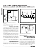
-100
-70
-80
-90
-60
-50
-40
-30
-20
-10
0
26 3028 3432 36 38
4-TONE MULTITONE POWER RATIO PLOT
(f
CLK
= 300MHz, f
CENTER
= 31.604MHz)
f
OUT
(MHz)
OUTPUT POWER (dBm)
f
T2
f
T3
f
T4
f
T1
A
OUT
= -12dB FS
BW = 12MHz
f
T1
= 29.6997MHz
f
T2
= 30.7251MHz
f
T3
= 32.4829MHz
f
T4
= 34.0209MHz
Figure 12. 4-Tone MTPR Test Results
**Thermal efficiency is not the key factor, since the MAX5886 features low-power operation. The exposed pad is the key element to
ensure a solid ground connection between the DAC and the PC board’s analog ground layer.