
Manual


MAX5886
3.3V, 12-Bit, 500Msps High Dynamic
Performance DAC with Differential LVDS Inputs
16 ______________________________________________________________________________________
In this package, the data converter die is attached to
an EP lead frame with the back of this frame exposed at
the package bottom surface, facing the PC board side
of the package. This allows a solid attachment of the
package to the PC board with standard infrared (IR)
flow soldering techniques. A specially created land pat-
tern on the PC board, matching the size of the EP (6mm
✕ 6mm), ensures the proper attachment and grounding
of the DAC. Designing vias*** into the land area and
implementing large ground planes in the PC board
design allow for highest performance operation of the
DAC. An array of at least 4 ✕ 4 vias (≤0.3mm diameter
per via hole and 1.2mm pitch between via holes) is rec-
ommended for this 68-pin QFN-EP package.
Static Performance Parameter Definitions
Integral Nonlinearity (INL)
Integral nonlinearity is the deviation of the values on an
actual transfer function from either a best straight line fit
(closest approximation to the actual transfer curve) or a
line drawn between the end points of the transfer func-
tion, once offset and gain errors have been nullified. For
a DAC, the deviations are measured at every individual
step.
Differential Nonlinearity (DNL)
Differential nonlinearity is the difference between an
actual step height and the ideal value of 1 LSB. A DNL
error specification of less than 1 LSB guarantees no
missing codes and a monotonic transfer function.
Offset Error
The offset error is the difference between the ideal and
the actual offset current. For a DAC, the offset point is
the average value at the output for the two midscale
digital input codes with respect to the full scale of the
DAC. This error affects all codes by the same amount.
Gain Error
A gain error is the difference between the ideal and the
actual full-scale output voltage on the transfer curve,
after nullifying the offset error. This error alters the slope
of the transfer function and corresponds to the same
percentage error in each step.
Settling Time
The settling time is the amount of time required from the
start of a transition until the DAC output settles its new
output value to within the converter’s specified accuracy.
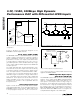
FERRITE BEAD
AV
CC
1µF10µF47µF
ANALOG POWER-SUPPLY
SOURCE
FERRITE BEAD
DV
CC
1µF10µF47µF
DIGITAL POWER-SUPPLY
SOURCE
FERRITE BEAD
VCLK
1µF10µF47µF
CLOCK POWER-SUPPLY
SOURCE
AV
DD
AGND
MAX5886
B0–B11
12
0.1µF
DGND
0.1µF
VCLK
CLKGND
0.1µF
OUTP
OUTN
DV
DD
BYPASSING—DAC LEVEL BYPASSING—BOARD LEVEL
Figure 13. Recommended Power-Supply Decoupling and Bypassing Circuitry
***Vias connect the land pattern to internal or external copper planes. It is important to connect as many vias as possible to the analog
ground plane to minimize inductance.