
Manual

MAX5886
3.3V, 12-Bit, 500Msps High Dynamic
Performance DAC with Differential LVDS Inputs
2 _______________________________________________________________________________________
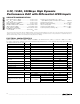
ABSOLUTE MAXIMUM RATINGS
ELECTRICAL CHARACTERISTICS
(AV
DD
= DV
DD
= VCLK = 3.3V, AGND = DGND = CLKGND = 0, external reference, V
REFIO
= 1.25V, R
L
= 50Ω, I
OUT
= 20mA,
T
A
= T
MIN
to T
MAX
, unless otherwise noted. ≥+25°C guaranteed by production test, <+25°C guaranteed by design and characteriza-
tion. Typical values are at T
A
= +25°C.)
Stresses beyond those listed under “Absolute Maximum Ratings” may cause permanent damage to the device. These are stress ratings only, and functional
operation of the device at these or any other conditions beyond those indicated in the operational sections of the specifications is not implied. Exposure to
absolute maximum rating conditions for extended periods may affect device reliability.
AV
DD
, DV
DD
, VCLK to AGND................................-0.3V to +3.9V
AV
DD
, DV
DD
, VCLK to DGND ...............................-0.3V to +3.9V
AV
DD
, DV
DD
, VCLK to CLKGND ...........................-0.3V to +3.9V
AGND, CLKGND to DGND....................................-0.3V to +0.3V
DACREF, REFIO, FSADJ to AGND.............-0.3V to AV
DD
+ 0.3V
IOUTP, IOUTN to AGND................................-1V to AV
DD
+ 0.3V
CLKP, CLKN to CLKGND...........................-0.3V to VCLK + 0.3V
B0P/B0N–B11P/B11N, SEL0,
PD to DGND...........................................-0.3V to DV
DD
+ 0.3V
Continuous Power Dissipation (T
A
= +70°C)
68-Pin QFN-EP (derate 41.7mW/°C above +70°C) ......3333mW
Thermal Resistance (θ
JA
) ..............................................+24°C/W
Operating Temperature Range ..........................-40°C to +85°C
Junction Temperature .....................................................+150°C
Storage Temperature Range ............................-60°C to +150°C
Lead Temperature (soldering, 10s) ................................+300°C
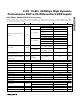
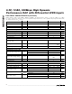
PARAMETER SYMBOL CONDITIONS MIN TYP MAX UNITS
STATIC PERFORMANCE
Resolution 12 Bits
Integral Nonlinearity INL Measured differentially ±0.2 LSB
Differential Nonlinearity DNL Measured differentially ±0.15 LSB
Offset Error OS -0.025 ±0.01 +0.025 %FS
Offset Drift ±50 ppm/°C
Full-Scale Gain Error GE
FS
External reference, T
A
≥ +25°C -3.5 +1.5 %FS
Internal reference ±100
Gain Drift
External reference ±50
ppm/°C
Full-Scale Output Current I
OUT
(Note 1) 2 20 mA
Min Output Voltage Single ended -0.5 V
Max Output Voltage Single ended 1.1 V
Output Resistance R
OUT
1MΩ
Output Capacitance C
OUT
5pF
DYNAMIC PERFORMANCE
Output Update Rate f
CLK
1 500 Msps
f
CLK
= 100MHz f
OUT
= 16MHz, -12dB FS -151
Noise Spectral Density
f
CLK
= 200MHz f
OUT
= 80MHz, -12dB FS -154
dB FS/
Hz
f
OUT
= 1MHz, 0dB FS 88
f
OUT
= 1MHz, -6dB FS 86
Spurious-Free Dynamic Range to
Nyquist
SFDR f
CLK
= 100MHz
f
OUT
= 1MHz, -12dB FS 80
dBc