
Manual

MAX5886
3.3V, 12-Bit, 500Msps High Dynamic
Performance DAC with Differential LVDS Inputs
_______________________________________________________________________________________ 7
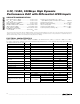
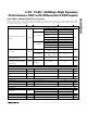
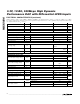
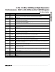
Pin Description
PIN NAME FUNCTION
1–8, 23, 34,
35–38
N.C. Not connected. Do not connect to these pins. Do not tie these pins together.
9, 41, 60, 62 DGND Digital Ground
10, 40, 61 DV
DD
Digital Supply Voltage. Accepts a supply voltage range of 3.135V to 3.465V. Bypass each pin with a
0.1µF capacitor to the nearest DGND.
11, 16 VCLK
Clock Supply Voltage. Accepts a supply voltage range of 3.135V to 3.465V. Bypass each pin with a
0.1µF capacitor to the nearest CLKGND.
12, 15 CLKGND Clock Ground
13 CLKP Converter Clock Input. Positive input terminal for LVDS-compatible differential converter clock.
14 CLKN
Complementary Converter Clock Input. Negative input terminal for the LVDS-compatible differential
converter clock.
17 PD
Power-Down Input. PD pulled high enables the DAC’s power-down mode. PD pulled low allows for
normal operation of the DAC. This pin features an internal pulldown resistor.
18, 24, 29,
30, 32
AV
DD
Analog Supply Voltage. Accepts a supply voltage range of 3.135V to 3.465V. Bypass each pin with a
0.1µF capacitor to the nearest AGND.
19, 25, 28,
31, 33, EP
AGND Analog Ground. Exposed paddle (EP) must be connected to AGND.
20 REFIO
Reference I/O. Output of the internal 1.2V precision bandgap reference. Bypass with a 1µF capacitor
to AGND. Can be driven with an external reference source.
21 FSADJ
Full-Scale Adjust Input. This input sets the full-scale output current of the DAC. For 20mA full-scale
output current, connect a 2kΩ resistor between FSADJ and DACREF.
22 DACREF
Return Path for the Current Set Resistor. For 20mA full-scale output current, connect a 2kΩ resistor
between FSADJ and DACREF.
26 IOUTN
Complementary DAC Output. Negative terminal for differential current output. The full-scale output
current range can be set from 2mA to 20mA.
27 IOUTP
DAC Output. Positive terminal for differential current output. The full-scale output current range can
be set from 2mA to 20mA.
39 SEL0
Mode Select Input SEL0. Set high to activate the segment shuffling function. Since this pin features an
internal pulldown resistor, it can be left open or pulled low to disable the segment-shuffling function.
See Segment Shuffling in the Detailed Description section for more information.
42 B11P Data Bit 11 (MSB)
43 B11N Complementary Data Bit 11 (MSB)
44 B10P Data Bit 10
45 B10N Complementary Data Bit 10
46 B9P Data Bit 9