
Owner manual


MAX5927/MAX5929
Low-Voltage, Quad, Hot-Swap
Controllers/Power Sequencers
4 _______________________________________________________________________________________
ELECTRICAL CHARACTERISTICS (continued)
(V
IN_
= +1V to +13.2V provided at least one supply is larger than or equal to +2.7V and only one supply is > +11.0V, T
A
= -40°C to
+85°C, unless otherwise noted. Typical values are at V
IN1
= 12.0V, V
IN2
= 5.0V, V
IN3
= 3.3V, V
IN4
= 1.0V, V
ON_
= +3.3V, and
T
A
= +25°C.) (Notes 1, 2)
PARAMETER SYMBOL CONDITIONS MIN TYP MAX UNITS
MODE Input Impedance R
MODE
200 kΩ
Autoretry Delay t
RETRY
Delay time to restart after fault shutdown
64 x
t
START
ms
Note 2: All devices are 100% tested at T
A
= +25°C. Limits over temperature are guaranteed by design.
Note 3: The slow-comparator threshold is adjustable. V
SC,TH
= R
LIM
x 7.5µA + 25mV (see the Typical Operating Characteristics).
Note 4: The current-limit slow-comparator response time is weighed against the amount of overcurrent—the higher the overcurrent
condition, the faster the response time (see the Typical Operating Characteristics).
Note 5: The startup period (t
START
) is the time during which the slow comparator is ignored and the device acts as a current limiter
by regulating the sense current with the fast comparator (see the Startup Period section).
Note 6: The current available at GATE is a function of V
GATE
(see the Typical Operating Characteristics).
Note 7: After a fault triggered by the fast comparator, the gate is discharged by the strong discharge current.
Note 8: Each channel input while the other inputs are at +1V.
Note 9: Each channel input while any other input is at +2.7V.
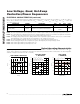
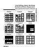
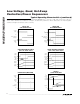
Typical Operating Characteristics
(Typical Operating Circuits, Q1 = Q2 = Q3 = Q4 = Fairchild FDB7090L, V
IN1
= 12V, V
IN2
= 5.0V, V
IN3
= 3.3V, V
IN4
= 1.0V, T
A
=
+25°C, unless otherwise noted. Channels 1 through 4 are identical in performance. Where characteristics are interchangeable,
channels 1 through 4 are referred to as W, X, Y, and Z.)
0
1
2
3
4
SUPPLY CURRENT vs. INPUT VOLTAGE
MAX5927 toc01
V
INW
(V)
I
IN
(mA)
0682 4 10 12 14
V
INX
= V
INY
= V
INZ
= 2.7V
I
INW
+ I
INX
+ I
INY
+ I
INZ
I
INW
I
INX
+ I
INY
+ I
INZ
1.0
1.5
2.0
2.5
3.0
3.5
4.0
4.5
5.0
264 8 10 12 14
TOTAL SUPPLY CURRENT
vs. INPUT VOLTAGE
MAX5927 toc02
V
IN
(V)
I
IN
(mA)
I
IN
= I
IN1
+ I
IN2
+ I
IN3
+ I
IN4
V
IN
= V
INW
= V
INX
= V
INY =
V
INZ
V
ON
= V
ON1
= V
ON2
= V
ON3
= V
ON4
V
ON
= 0V
V
ON
= 3.3V
0
1.0
0.5
2.0
1.5
2.5
3.0
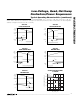
-40 85
SUPPLY CURRENT
vs. TEMPERATURE
MAX5927 toc03
TEMPERATURE (
°
C)
I
IN
(mA)
10-15 35 60
V
ON_
= V
INX
= V
INY
= V
INZ
= 2.7V
V
INW
= 2.8V
I
INW
+
I
INX
+ I
INY
+ I
INZ
I
INX
+ I
INY
+ I
INZ
I
INW