9-4167; Rev 0; 6/08 KIT ATION EVALU E L B AVAILA 0 to 16V, Quad, Hot-Swap Controller with 10-Bit Current and Voltage Monitor Features The MAX5961 0 to 16V, quad, hot-swap controller provides complete protection for systems with up to four distinct supply voltages. The device allows the safe insertion and removal of circuit cards into live backplanes. The MAX5961 is an advanced hot-swap controller that monitors voltage and current with an internal 10-bit ADC.
MAX5961 0 to 16V, Quad, Hot-Swap Controller with 10-Bit Current and Voltage Monitor ABSOLUTE MAXIMUM RATINGS IN, SENSE_, MON_, GATE_ to AGND ....................-0.3V to +30V PG_, ON_, FAULT_, SDA, SCL, ALERT, REG, DREG, POL, RETRY, HWEN .........................-0.3V to +6V DREG to REG ........................................................-0.3V to +0.3V ILIM_, MODE, PROT, A0, A1 ....................-0.3V to (VREG + 0.3V) GATE_ to MON_ (same channel) .............................-0.
0 to 16V, Quad, Hot-Swap Controller with 10-Bit Current and Voltage Monitor (VIN = 2.7V to 16V, TA = -40°C to +85°C, unless otherwise noted. Typical values are at VIN = 3.3V and TA = +25°C.) (Note 1) PARAMETER SYMBOL VMON_ = 0mV Current Measurement Error, 25mV Range VMON_ = 2.5V to 16V VMON_ = 0mV Current Measurement Error, 50mV Range (Note 2) VMON_ = 2.5V to 16V VMON_ = 0mV Current Measurement Error, 100mV Range (Note 2) VMON_ = 2.
MAX5961 0 to 16V, Quad, Hot-Swap Controller with 10-Bit Current and Voltage Monitor ELECTRICAL CHARACTERISTICS (continued) (VIN = 2.7V to 16V, TA = -40°C to +85°C, unless otherwise noted. Typical values are at VIN = 3.3V and TA = +25°C.) (Note 1) PARAMETER Slow Current-Limit Response Time SYMBOL tSCD CONDITIONS MIN TYP Overdrive = 4% of current-sense range 2.4 Overdrive = 8% of current-sense range 1.2 Overdrive = 16% of current-sense range 0.
0 to 16V, Quad, Hot-Swap Controller with 10-Bit Current and Voltage Monitor (VIN = 2.7V to 16V, TA = -40°C to +85°C, unless otherwise noted. Typical values are at VIN = 3.3V and TA = +25°C.) (Note 1) PARAMETER SYMBOL CONDITIONS MIN TYP MAX UNITS 400 kHz I2C INTERFACE Serial-Clock Frequency fSCL Bus Free Time Between STOP and START Condition tBUF 1.3 µs START Condition Setup Time tSU:STA 0.6 µs START Condition Hold Time tHD:STA 0.6 µs STOP Condition Setup Time tSU:STO 0.
Typical Operating Characteristics (continued) (VS_ = 12V, VIN = 3.3V, TA = +25°C, unless otherwise noted. See the Typical Application Circuit.) 9 8 IGATE_ (μA) 5.2 5.0 4.8 VMON_ = 12V IGATE_ (mA) 7 5.4 6 5 4 3 4.6 4.4 2 GATE_ DRIVE VOLTAGE REFERRED TO MON_ INPUT VOLTAGE 4.2 1 0 4.0 2 4 6 8 10 12 14 0 0.5 1.0 1.5 2.0 2.5 3.0 3.5 4.0 4.5 5.0 0.5 1.0 1.5 2.0 2.5 3.0 3.5 4.0 4.5 5.0 SLOW-COMPARATOR TURN-OFF TIME vs. SENSE VOLTAGE OVERDRIVE SLOW-COMPARATOR THRESHOLD VOLTAGE ERROR vs.
0 to 16V, Quad, Hot-Swap Controller with 10-Bit Current and Voltage Monitor TURN-OFF WAVEFORM (FAST COMPARATOR FAULT/SHORT-CIRCUIT RESPONSE) 4.0 DEFAULT RESISTOR SETTINGS 25mV SENSE RANGE CIRCULAR BUFFER CONTENT AT SLOW-TRIP FAULT 3.5 VGATE_, VMON_ CURRENT BUFFER (A) ILOAD_ MAX5961 toc13a CURRENT BUFFER vs. TIME MAX5961 toc12 3.0 2.5 2.0 1.5 1.0 VFAULT_ 0.5 0 -2.5 -2.0 -1.5 -1.0 -0.5 0 100μs/div 0.5 1.0 1.5 2.0 2.5 TIME (ms) VOLTAGE BUFFER vs.
Typical Operating Characteristics (continued) (VS_ = 12V, VIN = 3.3V, TA = +25°C, unless otherwise noted. See the Typical Application Circuit.) CURRENT BUFFER vs. TIME MAX5961 toc17b CURRENT DATA AT SHORT CIRCUIT ON POWER-UP 3 VOLTAGE BUFFER vs. TIME 5.0 MAX5961 toc17a 4 VOLTAGE DATA AT SHORT CIRCUIT ON POWER-UP 4.5 4.0 2 VOLTAGE BUFFER (V) 1 0 -1 3.5 3.0 2.5 2.0 1.5 1.0 -2 0.5 -3 0 -2.5 -2.0 -1.5 -1.0 -0.5 0 0.5 1.0 1.5 2.0 2.5 -2.5 -2.0 -1.5 -1.0 -0.5 0 0.5 1.0 1.5 2.0 2.
0 to 16V, Quad, Hot-Swap Controller with 10-Bit Current and Voltage Monitor PIN 1 NAME SENSE1 FUNCTION Channel 1 Current-Sense Input. Connect SENSE1 to the source of an external MOSFET and to one end of RSENSE1 (see the Typical Application Circuit). 2 MON1 Channel 1 Voltage Monitoring Input 3 GATE1 Channel 1 Gate-Drive Output. Connect to gate of an external n-channel MOSFET. 4 GND1 Channel 1 Gate Discharge Current Ground Return.
0 to 16V, Quad, Hot-Swap Controller with 10-Bit Current and Voltage Monitor MAX5961 Pin Description (continued) 10 PIN NAME FUNCTION 29 SENSE4 30 MON4 31 GATE4 Channel 4 Gate-Drive Output. Connect to gate of an external n-channel MOSFET. 32 GND4 Channel 4 Gate Discharge Current Ground Return. Connect all GND_ and DGND to AGND externally using a star connection. 33 GND2 Channel 2 Gate Discharge Current Ground Return. Connect all GND_ and DGND to AGND externally using a star connection.
0 to 16V, Quad, Hot-Swap Controller with 10-Bit Current and Voltage Monitor DREG MAX5961 4 SLOW FAULT_ FROM CONFIGURATION REGISTERS 4 RATIO FAST PG_ CIRCUITBREAKER DAC 4 4 SENSE_ ON_ HWEN RETRY 4 MON_ DEVICE CONTROL LOGIC VOLTAGE SCALER AND MULTIPLEXER 500mA MODE POL PROT ALERT 4 GATE_ CHARGE PUMP 4 ILIM_ UVLO SDA REGISTER BANK SCL I2C A0 IN REG LDO REF/BIAS AGND DGND 10-BIT ADC CIRCULAR BUFFER A1 GND1, GND2, GND3, GND4 __________________________________________________________
0 to 16V, Quad, Hot-Swap Controller with 10-Bit Current and Voltage Monitor MAX5961 Typical Operating Circuit VDD μC VDD VDD VS4* VS2* 4 ON2 SCL ALERT FAULT_ A0 A1 IN SDA SCL SDA 4 ID SETTING ON1 INT I/O PG_ 2.
0 to 16V, Quad, Hot-Swap Controller with 10-Bit Current and Voltage Monitor VDD μC SCL VDD SDA I/O I/O INT VDD 3.9kΩ 100kΩ VS3* VS1* 2.7V TO 16V VS2* ID SETTING 4 4 100kΩ VS4* 3.
MAX5961 0 to 16V, Quad, Hot-Swap Controller with 10-Bit Current and Voltage Monitor Detailed Description The MAX5961 0 to 16V, quad, hot-swap controller provides complete protection for multisupply systems. The device allows the safe insertion and removal of circuit cards into live backplanes. The MAX5961 is an advanced hot-swap controller that monitors voltage and current with an internal 10-bit ADC.
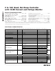
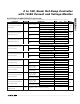
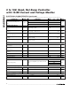
0 to 16V, Quad, Hot-Swap Controller with 10-Bit Current and Voltage Monitor REGISTER DESCRIPTION ADDRESS (HEX CODE) CHANNEL 1 CHANNEL 2 CHANNEL 3 CHANNEL 4 RESET VALUE TABLE uv1_chx_h High 8 bits ([9:2]) of undervoltage warning (UV1) threshold 0x32 0x3C 0x46 0x50 0x00 21 uv1_chx_l Low 2 bits ([1:0]) of undervoltage warning (UV1) threshold 0x33 0x3D 0x47 0x51 0x00 22 uv2_chx_h High 8 bits ([9:2]) of undervoltage critical (UV2) threshold 0x34 0x3E 0x48 0x52 0x00 23 uv2_chx_l
MAX5961 0 to 16V, Quad, Hot-Swap Controller with 10-Bit Current and Voltage Monitor Table 1b. Register Address Map (General) REGISTER DESCRIPTION ADDRESS (HEX CODE) RESET VALUE TABLE mon_range MON_ input range selection 0x30 0x00 17, 18 cbuf_chx_store Selective enabling of individual blocks in the circular buffer 0x31 0xFF 42 ifast2slow Current threshold ratio setting for the fast comparator vs.
0 to 16V, Quad, Hot-Swap Controller with 10-Bit Current and Voltage Monitor The inputs ON_ and Chx_EN2 can be set externally; the initial state of the Chx_EN2 bits in register chxen is set by the state of the HWEN input when IN rises above VUVLO. The ON_ inputs connect to internal precision analog comparators with a 0.6V threshold. Whenever VON_ is above 0.6V, the corresponding ON_ bit in register status1[3:0] is set to 1.
MAX5961 0 to 16V, Quad, Hot-Swap Controller with 10-Bit Current and Voltage Monitor Table 4b.
0 to 16V, Quad, Hot-Swap Controller with 10-Bit Current and Voltage Monitor pation is therefore roughly equivalent to a single pulse of magnitude (VS_ x I_INRUSH)/2 and duration tSU. Refer to the thermal resistance charts in the MOSFET data sheet to determine the junction temperature rise during startup, and ensure that this does not exceed the maximum junction temperature for worst-case ambient conditions.
2.0 25mV SENSE RANGE; DAC = 191, VTH,ST = 9.36mV 1.8 1.6 MAX5961 fig02 The fast-trip threshold is always higher than the slow-trip threshold, and the fast-trip comparator responds very quickly to protect the system against sudden, severe overcurrent events. The slower response of the slow-trip comparator varies depending upon the amount of overdrive beyond the slow-trip threshold. If the overdrive is small and short-lived, the comparator will not shut down the affected channel.
0 to 16V, Quad, Hot-Swap Controller with 10-Bit Current and Voltage Monitor operation and fault-management flowchart for one channel of the MAX5961. Table 6.
MAX5961 0 to 16V, Quad, Hot-Swap Controller with 10-Bit Current and Voltage Monitor READ MODE, PROT, A0, A1, RETRY, HWEN, ILIM_ INPUTS, CLEAR FLAGS VIN > 2.7V ARE 2 OR MORE OF 3 ENABLE SET? CHANNEL ENABLED NO NO START CIRCULAR BUFFER ENABLE GATE_ PULLUP CONTINUOUSLY SAMPLE VOLTAGE AND CURRENT, UPDATE MIN-MAX VALUES, HANDLE I2C COMMUNICATIONS, STORE SAMPLES TO CIRCULAR BUFFERS...
0 to 16V, Quad, Hot-Swap Controller with 10-Bit Current and Voltage Monitor Description: Fast-comparator threshold DAC setting Register Titles: dac_ch1 dac_ch2 dac_ch3 dac_ch4 Register Addresses: 0x5A 0x5B 0x5C 0x5D R/W R/W R/W R/W R/W R/W R/W R/W bit 7 bit 6 bit 5 bit 4 bit 3 bit 2 bit 1 bit 0 RESET VALUE 0xBF Digital Current Monitoring used throughout the MAX5961 for all 10-bit ADC conversion results and 10-bit digital comparator thresholds.
MAX5961 0 to 16V, Quad, Hot-Swap Controller with 10-Bit Current and Voltage Monitor Table 11. Overcurrent Warning Threshold Register Format (High-Order Bits) Description: Overcurrent warning threshold, high-order bits [9:2] Register Titles: oc_ch1_h oc_ch2_h oc_ch3_h oc_ch4_h Register Addresses: 0x3A 0x44 0x4E 0x58 R/W R/W R/W R/W R/W R/W R/W R/W RESET VALUE oc_9 oc_8 oc_7 oc_6 oc_5 oc_4 oc_3 oc_2 0xFF bit 7 bit 6 bit 5 bit 4 bit 3 bit 2 bit 1 bit 0 Table 12.
0 to 16V, Quad, Hot-Swap Controller with 10-Bit Current and Voltage Monitor Description: Minimum current conversion result, low-order bits [1:0] Register Titles: min_ch1_cs_l min_ch2_cs_l min_ch3_cs_l min_ch4_cs_l Register Addresses: 0x11 0x19 0x21 0x29 R/W R/W bit 7 R/W bit 6 bit 5 R/W bit 4 R/W R/W bit 3 bit 2 R/W R/W RESET VALUE imin_1 imin_0 0x03 bit 1 bit 0 Table 15.
MAX5961 0 to 16V, Quad, Hot-Swap Controller with 10-Bit Current and Voltage Monitor Digital Voltage Monitoring and Power-Good Outputs register mon_range. The default range is 16V (Tables 17 and 18). The most recent voltage conversion results can be read from the adc_chx_mon_h and adc_chx_mon_l registers (see Tables 19 and 20). The voltage at the load (MON_ inputs) is sampled by the internal ADC. The MON_ full-scale voltage for each channel can be set to 16V, 8V, 4V, or 2V by writing to Table 17.
0 to 16V, Quad, Hot-Swap Controller with 10-Bit Current and Voltage Monitor undervoltage (UV) levels (see Tables 21–24) and two overvoltage (OV) levels (see Tables 25–28). Table 21.
MAX5961 0 to 16V, Quad, Hot-Swap Controller with 10-Bit Current and Voltage Monitor Table 25.
0 to 16V, Quad, Hot-Swap Controller with 10-Bit Current and Voltage Monitor it only determines the system response to the critical digital comparators (see Tables 4a, 4b, and 29). In a typical application, the UV1 and OV1 thresholds would be set closer to the nominal output voltage, and the UV2 and OV2 thresholds would be set further from nominal (see Figure 4). This provides a “progressive” response to a voltage excursion.
MAX5961 0 to 16V, Quad, Hot-Swap Controller with 10-Bit Current and Voltage Monitor Power-Good Detection and PG_ Outputs The PG_ output for a given channel is asserted when the voltage at MON_ is between the undervoltage and overvoltage critical limits. The status of the power-good signals is maintained in register status3[3:0]. A value of 1 in any of the pg[] bits indicates a power-good condition, regardless of the POL setting, which only affects the PG_ output polarity.
0 to 16V, Quad, Hot-Swap Controller with 10-Bit Current and Voltage Monitor These peak detection registers are read/write accessible through the I2C interface (see Tables 32–35). The minimum-value registers are reset to 0x3FF, and the maximum-value registers are reset to 0x000. These reset values are loaded upon startup of a channel or at any time as commanded by register peak_log_rst (see Table 36). Table 32.
MAX5961 0 to 16V, Quad, Hot-Swap Controller with 10-Bit Current and Voltage Monitor Table 35.
0 to 16V, Quad, Hot-Swap Controller with 10-Bit Current and Voltage Monitor by the particular compare and the setting of the PROT input. The deglitching function is enabled or disabled per comparator by registers dgl_i, dgl_uv, and dgl_ov (Tables 38, 39, and 40). Writing a 1 to the appropriate bit location in these registers enables the deglitch function for the corresponding digital comparator. Table 38.
MAX5961 0 to 16V, Quad, Hot-Swap Controller with 10-Bit Current and Voltage Monitor Circular Buffer The MAX5961 features eight 10-bit circular buffers (in volatile memory) that contain a history of the 50 mostrecent voltage and current digital conversion results for each hot-swap channel. These circular buffers can be read back through the I2C interface.
0 to 16V, Quad, Hot-Swap Controller with 10-Bit Current and Voltage Monitor The circular buffer system has a user-programmable “stop delay” that specifies a certain number of sample cycles to continue recording to the buffer after a shutdown occurs. This delay value is stored in register cbuf_dly_stop[5:0] (see Table 44).
MAX5961 0 to 16V, Quad, Hot-Swap Controller with 10-Bit Current and Voltage Monitor Table 45. Force-On Control Register Format Description: Force-on control register Register Title: foset Register Address: 0x68 R R R R R/W R/W R/W R/W RESET VALUE 0 0 0 0 ch4_fo ch3_fo ch2_fo ch1_fo 0x00 bit 7 bit 6 bit 5 bit 4 bit 3 bit 2 bit 1 bit 0 Table 46.
0 to 16V, Quad, Hot-Swap Controller with 10-Bit Current and Voltage Monitor Overvoltage digital-compare status register (warning [3:0] and critical [7:4] overvoltage event detection status) Description: Register Title: fault1 Register Address: 0x64 R/C R/C R/C R/C R/C R/C R/C R/C RESET VALUE ch4_ov2 ch3_ov2 ch2_ov2 ch1_ov2 ch4_ov1 ch3_ov1 ch2_ov1 ch1_ov1 0x00 bit 7 bit 6 bit 5 bit 4 bit 3 bit 2 bit 1 bit 0 Table 49.
MAX5961 0 to 16V, Quad, Hot-Swap Controller with 10-Bit Current and Voltage Monitor I2C Serial Interface ter device to generate a clock signal. The master device (typically a µC) initiates data transfer on the bus and generates SCL to permit that transfer. A master device communicates to the MAX5961 by transmitting the proper address followed by command and/or data words. Each transmit sequence is framed by a START (S) or REPEATED START (SR) condition and a STOP (P) condition.
0 to 16V, Quad, Hot-Swap Controller with 10-Bit Current and Voltage Monitor Early STOP Conditions The MAX5961 recognizes a STOP condition at any point during transmission except if a STOP condition occurs in the same high pulse as a START condition. This condition is not a legal I2C format. At least one clock pulse must separate any START and STOP condition. START and STOP Conditions Both SCL and SDA idle high when the bus is not busy.
MAX5961 0 to 16V, Quad, Hot-Swap Controller with 10-Bit Current and Voltage Monitor WRITE WORD FORMAT SEND BYTE FORMAT S ADDRESS WR 7 BITS 0 ACK DATA ACK S P 8 BITS SLAVE ADDRESS– EQUIVALENT TO CHIPSELECT LINE OF A 3WIRE INTERFACE. DATA BYTE–PRESETS THE INTERNAL ADDRESS POINTER. ADDRESS WR 7 BITS 1 WR 7 BITS 0 ACK COMMAND ACK 8 BITS SLAVE ADDRESS– EQUIVALENT TO CHIPSELECT LINE OF A 3WIRE INTERFACE. DATA ACK 8 BITS COMMAND BYTE– MSB OF THE EEPROM REGISTER BEING WRITTEN.
0 to 16V, Quad, Hot-Swap Controller with 10-Bit Current and Voltage Monitor Send Byte The send byte protocol allows the master device to send one byte of data to the slave device (see Figure 8). The send byte presets a register pointer address for a subsequent read or write. The slave sends a NACK instead of an ACK if the master tries to send an address that is not allowed. If the master sends a STOP condition, the internal address pointer does not change.
MAX5961 0 to 16V, Quad, Hot-Swap Controller with 10-Bit Current and Voltage Monitor Receive Byte The receive byte protocol allows the master device to read the register content of the MAX5961 (see Figure 8). The EEPROM or register address must be preset with a send byte protocol first. Once the read is complete, the internal pointer increases by one. Repeating the receive byte protocol reads the contents of the next address. The receive byte procedure follows: 1) The master sends a START condition.