
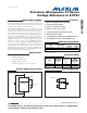
Owner manual
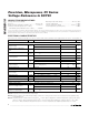


ABSOLUTE MAXIMUM RATINGS
Stresses beyond those listed under “Absolute Maximum Ratings” may cause permanent damage to the device. These are stress ratings only, and functional
operation of the device at these or any other conditions beyond those indicated in the operational sections of the specifications is not implied. Exposure to
absolute maximum rating conditions for extended periods may affect device reliability.
(Voltages Referenced to GND)
V
IN
, V
OUT
..................................................................-0.3V to +6V
Output Short-Circuit Duration to GND or V
IN
............Continuous
Continuous Power Dissipation (T
A
= +70°C)
3-Pin SOT23 (derate 4.0mW/°C above +70°C).............320mW
Operating Temperature Range ...........................-40°C to +85°C
Junction Temperature......................................................+150°C
Storage Temperature Range .............................-65°C to +150°C
Lead Temperature (soldering, 10s) .................................+300°C
MAX6010
Precision, Micropower, 3V Series
Voltage Reference in SOT23
2 _______________________________________________________________________________________
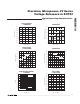
ELECTRICAL CHARACTERISTICS
(V
IN
= 5V; C
OUT
= 47nF, C
IN
= 0.1µF, I
OUT
= 0; T
A
= T
MIN
to T
MAX
, unless otherwise noted. Typical values are at T
A
= +25°C.) (Note 1)
PARAMETER SYMBOL CONDITIONS MIN TYP MAX UNITS
OUTPUT
MAX6010A (0.2%), T
A
= +25°C 2.994 3.000 3.006
Output Voltage V
OUT
MAX6010B (0.4%), T
A
= +25°C 2.988 3.000 3.012
V
Output-Voltage Temperature
Drift
TCV
OUT
(Note 2) 16 50 ppm/
o
C
Line Regulation
∆V
OUT
/
∆V
IN
3.2V ≤ V
IN
≤ 5.5V 50 350 µV/V
0 ≤ I
OUT
≤ 7mA 60 200 µV/mA
Load Regulation
∆V
OUT
/
∆I
OUT -1mA ≤ I
OUT
≤ 0 0.25 10 µV/µA
Sourcing to GND 20
Short-Circuit Current I
SC
Sinking from V
IN
15
mA
Dropout Voltage
V
IN
-
V
OUT
I
OUT
= 1mA (Note 3) 55 200 mV
Thermal Hysteresis (Note 4) 210 ppm
DYNAMIC CHARACTERISTICS
0.1Hz to 10Hz 100 µV
P-P
Noise Voltage e
OUT
10Hz to 10kHz 200 µV
RMS
Ripple Rejection PSRR V
IN
= 5V ±100mV (f ≤ 2kHz), I
OUT
= 1mA 50 dB
Turn-On Settling Time t
R
Settling to 0.1%, C
OUT
= 0.1µF 700 µs
Capacitive-Load Stability Range C
OUT
(Note 2) 1 1000 nF
INPUT
Supply Voltage Range V
IN
Guaranteed by line regulation test 3.2 5.5 V
T
A
= +25°C 3.6 5
Quiescent Supply Current I
IN
T
A
= T
MIN
to T
MAX
3.6 6
µA
Change in Quiescent Supply
Current vs. Input Voltage
∆I
IN
/∆V
IN
3.2V ≤ V
IN
≤ 5.5V 0.5 0.25 µA/V
Note 1: Devices are 100% production tested at T
A
= +25°C and are guaranteed by design from T
A
= T
MIN
to T
MAX
.
Note 2: Not production tested. Guaranteed by design.
Note 3: Dropout voltage is the minimum input voltage at which V
OUT
changes ≤ 0.2% from V
OUT
at rated V
IN
and is guaranteed by
load regulation test.
Note 4: Thermal hysteresis is defined as the change in T
A
= +25°C output voltage before and after temperature cycling of the device
(from T
A
= T
MIN
to T
MAX
). Initial measurement at T
A
= +25°C is followed by temperature cycling the device to T
A
= +85°C
then to T
A
= -40°C and another measurement at T
A
= +25°C is compared to the original measurement at T
A
= +25°C.