
Owner manual

MAX606/MAX607
Low-Profile, 5V/12V or Adjustable, Step-Up
DC-DC Converters for Flash Memory/PCMCIA Cards
10 ______________________________________________________________________________________
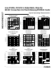
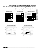
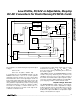
When FB is connected to IN or GND, an internal volt-
age divider is configured to produce a predetermined
output. However, when the voltage at FB is between
0.1V above ground and 0.1V below V
IN
, the device is in
the adjustable output mode. In this mode, the
MAX606/MAX607 output voltage is set by two external
resistors, R1 and R2 (Figure 4), which form a voltage
divider between the output and FB. Use the following
equation to determine the output voltage:
V
OUT
= V
REF
(R1 / R2 + 1)
where V
REF
= 2V. To simplify the resistor selection:
R1 = R2 [(V
OUT
/ V
REF
) - 1]
Since the input current at FB is 200nA maximum, large
values (up to 100kΩ) can be used for R2 with no signifi-
cant loss of accuracy. For 1% error, the current through
R2 should be at least 100 times the FB input bias current.
Soft-Start
Connecting a capacitor to the Soft-Start (SS) pin
ensures a gradually increasing current limit during
power-up or when exiting shutdown, thereby reducing
initial inrush currents. This feature can be useful, for
example, when an old battery’s increased series resis-
tance limits initial inrush currents. Using the soft-start
feature in a situation like this minimizes the risk of over-
loading the incoming supply.
Soft-start timing is controlled by the value of the SS
capacitor. On power-up, the SS capacitor is charged by
the 2V reference through an internal, 45kΩ pull-up resis-
tor. As the voltage on the SS pin increases, the voltage
at the SS clamp output also increases, which in turn
raises the current-limit threshold. The Start-Up Delay vs.
SS Capacitor graph in the
Typical Operating Charac-
teristics
shows typical timing characteristics for selected
capacitor values and circuit conditions. The soft-start
capacitor is discharged each time the MAX606 or
MAX607 is put into shutdown, including during under-
voltage lockout and when powering down at IN.
If the circuit is required to start up with no load, as in
flash memory programming supplies, soft-start is not
required. Omitting the soft-start capacitor permits a
minimum output voltage rise time from the shutdown
state, improving flash memory access time.
Undervoltage Lockout
The MAX606/MAX607 monitor the supply voltage at IN
and operate for supply voltages greater than 2.8V.
When an undervoltage condition is detected, control
logic turns off the output power FET and discharges the
soft-start capacitor to ground. The control logic holds
the output power FET in an off state until the supply
voltage rises above the undervoltage threshold, at
which time a soft-start cycle begins.
Shutdown Mode
Connecting SHDN to GND will hold the MAX606/
MAX607 in shutdown mode. In shutdown, the output
power FET is off, but there is still an external path from
IN to the load via the inductor and diode. The internal
reference also turns off, which causes the soft-start
capacitor to discharge. Typical device standby current
in shutdown mode is 0.01µA. For normal operation,
connect SHDN to IN. A soft-start cycle is initiated when
the MAX606/MAX607 exit shutdown.
Applications Information
Inductor Selection
Use a 5µH inductor for the MAX606 and a 10µH induc-
tor for the MAX607. See Table 3 for a list of component
suppliers. Higher inductor values allow greater load
currents due to operation in continuous-conduction
mode, while lower inductor values lead to smaller phys-
ical size due to lower energy-storage requirements and
lower output-filter-capacitor requirements. Potential
drawbacks of using lower inductor values are
increased output ripple, lower efficiency, and lower out-
put-current capability due to operation in discontinu-
ous-conduction mode. (See the Maximum Output
Current vs. Inductor Value graph in the
Typical
Operating Characteristics
.)
The inductor must have a saturation (incremental) cur-
rent rating equal to the peak switch-current limit, which
is 1.1A. For highest efficiency, minimize the inductor’s
DC resistance.
R1
10pF
R2
MAX606
MAX607
LX
FB
OUT
PGNDGND
IN
OUTPUT
INPUT
V
OUT
= V
REF
(
+ 1
)
R1
R2
V
REF
= 2V
Figure 4. Adjustable Output Voltage