
Owner manual
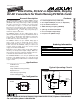

MAX606/MAX607
Low-Profile, 5V/12V or Adjustable, Step-Up
DC-DC Converters for Flash Memory/PCMCIA Cards
2 _______________________________________________________________________________________
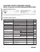
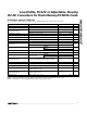
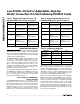
ABSOLUTE MAXIMUM RATINGS
ELECTRICAL CHARACTERISTICS
(V
IN
= 3.3V, GND = PGND = FB = 0V, SHDN = IN, T
A
= 0°C to +85°C, unless otherwise noted. Typical values are at T
A
= +25°C.)
Stresses beyond those listed under “Absolute Maximum Ratings” may cause permanent damage to the device. These are stress ratings only, and functional
operation of the device at these or any other conditions beyond those indicated in the operational sections of the specifications is not implied. Exposure to
absolute maximum rating conditions for extended periods may affect device reliability.
IN to GND.................................................................-0.3V to +6V
LX, OUT to GND.....................................................-0.3V to +15V
PGND to GND.....................................................................±0.3V
FB to GND..................................................-0.3V to (V
CC
+ 0.3V)
SS, SHDN
to GND....................................................-0.3V to +6V
Continuous Power Dissipation (T
A
= +70°C)
µMAX (derate 4.10mW/°C above +70°C) ....................330mW
SO (derate 5.88mW/°C above +70°C).........................471mW
Operating Temperature Range ...........................-40°C to +85°C
Storage Temperature.......................................................+160°C
Lead Temperature (soldering, 10sec).............................+300°C
V
IN
= 3V to 5.5V. For V
FB
below this voltage,
output regulates to 12V.
V
SHDN
= 0 or V
IN
3V < V
IN
< 5V, FB = IN, I
LOAD
= 0 to 180mA
V
IN
= 5.5V
V
IN
= 3V
2V < (V
OUT
+ 0.5V - V
IN
) < 8V (see
Pulse-
Frequency-Modulation Control Scheme
section)
3V < V
IN
< 5.5V
(t
ON
= K / V
IN
)
V
OUT
= 13V
V
SHDN
= V
IN
, V
SS
= 150mV
V
SHDN
= 0, OUT = IN
V
LX
= 12V
4.5V < V
IN
< 5.5V, FB = GND, I
LOAD
= 0 to 120mA
0.1V < V
FB
< (V
IN
- 0.1V)
0.1V < V
FB
< (V
IN
- 0.1V)
V
OUT
= 13V
V
IN
= 3V to 5.5V
V
SHDN
= V
SS
= 0
CONDITIONS
V0.1FB Input Low Voltage
µA±1
SHDN Input Current
V0.66V
IN
SHDN Input High Voltage
V0.25V
IN
SHDN Input Low Voltage
0.3 0.7Switch Off-Time Ratio
3.8 6.0 8.6
µs-A
1.9 3.0 4.3
Switch On-Time Constant (K)
µA80OUT Input Current
µA0.01 10Shutdown Quiescent Current
150 300
µA
250 500
Quiescent Supply Current
0.5
V
4.8 5.0 5.2
Output Voltage (Note 1)
V2.4 2.8
V3.0 5.5Supply Voltage
Undervoltage Lockout Threshold
kΩ
30 45 60
SS Resistance
A0.7 1.1Switch Current Limit
µA10Switch Off-Leakage
Ω
0.4 1Switch On-Resistance
11.5 12.0 12.5
V1.96 2.00 2.04FB Regulation Setpoint
VV
IN
12.5Adjustable Output Voltage Range
%0.5Line Regulation
UNITSMIN TYP MAXPARAMETER
V
IN
= 3V to 5.5V. For V
FB
above this voltage,
output regulates to 5V.
VV
IN
- 0.1FB Input High Voltage
V
FB
= 2.05V, V
OUT
= 13V nA200FB Input Current
MAX606
MAX607
MAX606
MAX607