
Owner manual

MAX606/MAX607
Low-Profile, 5V/12V or Adjustable, Step-Up
DC-DC Converters for Flash Memory/PCMCIA Cards
_______________________________________________________________________________________ 7
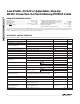
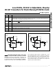
Pin Description
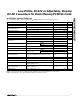
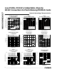
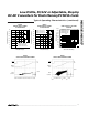
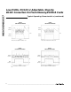
Standard Application Circuits
This data sheet provides two predesigned standard
application circuits. The circuit of Figure 1 produces 12V
at 120mA from a 5V input. Table 1 lists component val-
ues and part numbers for both the MAX606 and MAX607
variations of this circuit. The circuit of Figure 2 produces
5V at a typical output current of 180mA from a 3.3V
input. Each application circuit is designed to deliver the
full rated output load current over the temperature range
listed. Component values and part numbers for this cir-
cuit are listed in Table 2. See Table 3 for component
suppliers’ phone and fax numbers.
C1
C2
C3
D1
C4
MAX606
MAX607
LX
OUT
SHDN
SS
FB
GND
PGND
IN
ON/OFF OUTPUT
12V @ 120mA
+5V
INPUT
L1
C1
D1
L1
C2
C3
C4
MAX606
MAX607
LX
OUT
SHDN
SS
GND
PGND
INFB
ON/OFF OUTPUT
5V @ 180mA
+3.3V
INPUT
Figure 1. 12V Standard Application Circuit Figure 2. 5V Standard Application Circuit
NAME FUNCTION
1
PGND Power Ground. Source of n-channel power MOSFET.
2 FB
Feedback Input. Connect to IN for 5V output, to GND for 12V output, or to a resistive voltage divider between
OUT and GND for an adjustable output between IN and 12.5V.
PIN
3 SHDN
Shutdown Input, Active Low. Connect to GND to power down or to IN for normal operation. Output power FET
is held off when SHDN
is low.
4 IN Supply Voltage Input: 3.0V to 5.5V
8 LX Drain of n-channel power MOSFET
7 OUT Output. Always connect directly to the circuit output.
6 SS Soft-Start Input
5 GND Analog Ground