
Owner manual

MAX606/MAX607
Low-Profile, 5V/12V or Adjustable, Step-Up
DC-DC Converters for Flash Memory/PCMCIA Cards
_______________________________________________________________________________________ 9
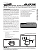
The on/off times are determined by the input and output
voltages:
t
ON
= K / V
IN
t
OFF
= 0.5 · K / (V
OUT
+ V
DIODE
- V
IN
)
K is typically 3µs-V for the MAX606 and 6µs-V for the
MAX607. This factor is chosen to set the optimum
switching frequency and the one-cycle current limit,
which determines the no-load output ripple at low out-
put-to-input voltage differentials. The factor of 0.5 in the
off-time equation is the typical switch off-time ratio. This
ratio guarantees high efficiency under a heavy load by
allowing the inductor to operate in continuous-conduc-
tion mode. For example, a switch off-time ratio of 1
would cause the device to operate on the edge of dis-
continuous-conduction mode.
To determine the actual switch off-time ratio for a par-
ticular device, measure t
ON
, t
OFF
, V
IN
, and V
OUT
, and
then solve for the ratio by substituting these values into
the off-time equation.
Unlike PWM converters, the MAX606/MAX607 generate
variable-frequency switching noise. However, the
amplitude of this noise does not exceed the product of
the switch current limit and the output capacitor equiva-
lent series resistance (ESR). Traditional clocked-PFM or
pulse-skipping converters cannot make this claim.
Output Voltage Selection
The MAX606/MAX607 output voltage is pin-program-
mable to 5V and 12V, and also adjustable to voltages
between V
IN
and 12.5V. Connect FB to IN for a 5V out-
put, to GND for a 12V output, or to a resistive divider
between the output and GND for an adjustable output.
Always connect OUT to the output.
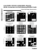
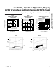
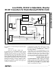
UNDER-
VOLTAGE
LOCKOUT
DUAL
MODE
REF
CURRENT-LIMIT
COMPARATOR
ERROR
COMPARATOR
TIMING CIRCUIT
t
ON
t
OFF
CONTROL
LOGIC
EN
ON
INH
OFF
SHDN
FB
INT/EXT
FB
5V/12V
OUT
SS
PGND
INTERNAL
POWER
1Ω SWITCH
LX
IN
V
REF
DRIVER
R
LIM
MAX606
MAX607
Figure 3. Functional Diagram