
Owner's manual
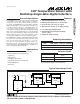

MAX6575L/H
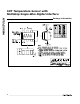
SOT Temperature Sensor with
Multidrop Single-Wire Digital Interface
2 _______________________________________________________________________________________
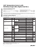
ABSOLUTE MAXIMUM RATINGS
ELECTRICAL CHARACTERISTICS
(V
DD
= +2.7V to +5.5V, T
A
= -40°C to +125°C, unless otherwise noted. Typical values are specified at T
A
= +25°C and V
DD
= +5V,
unless otherwise noted.)
Stresses beyond those listed under “Absolute Maximum Ratings” may cause permanent damage to the device. These are stress ratings only, and functional
operation of the device at these or any other conditions beyond those indicated in the operational sections of the specifications is not implied. Exposure to
absolute maximum rating conditions for extended periods may affect device reliability.
Note 1: See Temperature Accuracy histograms in
Typical Operating Characteristics
.
Note 2: Guaranteed by design. Not production tested.
Note 3: Limit maximum start pulse at 1ms to avoid timing overlap.
Note 4: If no reset pulse is applied.
Terminal Voltage (with respect to GND)
V
DD
........................................................................-0.3V to +6V
TS1, TS0..................................................-0.3V to (V
DD
+ 0.3V)
I/O..........................................................................-0.3V to +6V
Input/Output Current, All Pins...........................................±20mA
Continuous Power Dissipation (T
A
= +70°C)
6-Pin SOT23 (derate 7.10mW/°C above +70°C)...........571mW
Operating Temperature Range .........................-40°C to +125°C
Storage Temperature Range.............................-65°C to +150°C
Lead Temperature (soldering, 10sec).............................+300°C
V
DD
= 5.5V
V
DD
> 2.7V, I
SINK
= 1.2mA
V
DD
> 4.5V, I
SINK
= 3.2mA
Figure 1
Figure 1
Figure 1
Figure 1, T
A
= +25°C
CONDITIONS
V2.3V
IH
I/O Input Voltage High
V0.8V
IL
I/O Input Voltage Low
V
0.3
V
OL
I/O Output Voltage Low
0.4
2.3V
IH
Time-Select Pin Logic Levels V
0.8V
IL
ns500Glitch Immunity on I/O Input
ms520t
READY
Delay Time from Trigger to
Ready (Note 4)
µs2.5t
START
Start Pulse (Note 3)
-7.5 ±1.1 +7.5
µA
150 250
I
DD
V2.7 5.5V
DD
V
DD
Range
Supply Current
µs10t
SETUP
Setup Time
µs5Tt
L1-8
Output Pulse Low Time
5Tt
D1
°C
Temperature Sensor Error
(Note 1)
-5.5 ±0.9 +5.5
-3.0 ±0.8 +3.0
-4.5 ±0.5 +4.5
-5.0 ±0.5 +5.0
UNITSMIN TYP MAXSYMBOLPARAMETER
T
A
= -20°C
T
A
= 0°C
T
A
= +25°C
T
A
= +85°C
T
A
= +125°C
Figure 1 ms4.6 16.0t
RESET
Reset Pulse Width (Note 2)
V
TS1
= GND, V
TS0
= GND
V
TS1
= GND, V
TS0
= V
DD
20Tt
D2
V
TS1
= V
DD
, V
TS0
= GND
MAX6575L,
T (temp) in °K,
Figure 1
40Tt
D3
Output Pulse Delay
V
TS1
= V
DD
, V
TS0
= V
DD
80Tt
D4
V
TS1
= GND, V
TS0
= GND 160Tt
D5
V
TS1
= GND, V
TS0
= V
DD
320Tt
D6
V
TS1
= V
DD
, V
TS0
= GND
MAX6575H,
T (temp) in °K,
Figure 1
480Tt
D7
V
TS1
= V
DD
, V
TS0
= V
DD
µs
640Tt
D8
T
A
= -40°C to +85°C
T
A
= -40°C to +125°C 400