
User guide
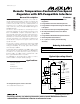

MAX6661
5) When introducing a thermocouple by inserting differ-
ent metals in the connection path, make sure that
both the DXP and the DXN paths have matching
thermocouples, i.e., the connection paths are sym-
metrical. A copper-solder thermocouple exhibits
3µV/°C. Adding a few thermocouples causes a neg-
ligible error.
6) The 10mil widths and spacings that are recommend-
ed in Figure 2 are not absolutely necessary, as they
offer only a minor improvement in leakage and noise
over narrow traces. Use wider traces when practical.
7) Add a 5Ω resistor in series with V
CC
for best noise
filtering (see Typical Operating Circuit).
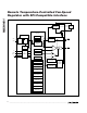
PC Board Layout Checklist
• Place the MAX6661 close to the remote-sense junc-
tion.
• Keep traces away from high voltages (12V bus).
• Keep traces away from fast data buses and CRTs.
• Use recommended trace widths and spacings.
• Place a ground plane under the traces.
• Use guard traces connected to GND flanking DXP
and DXN.
• Place the noise filter and the 0.1µF V
CC
bypass
capacitors close to the MAX6661.
Twisted-Pair and Shielded Cables
Use a twisted-pair cable to connect the remote sensor
for distances longer than 8in or in very noisy environ-
ments. Twisted-pair cable lengths can be between 6ft
and 12ft before noise introduces excessive errors. For
longer distances, the best solution is a shielded twisted
pair like that used for audio microphones. For example,
Belden 8451 works well for distances up to 100ft in a
noisy environment. At the device, connect the twisted
pair to DXP and DXN and the shield to GND. Leave the
shield unconnected at the remote sensor. For very long
cable runs, the cable’s parasitic capacitance often pro-
vides noise filtering, so the 2200pF capacitor can often
be removed or reduced in value. Cable resistance also
affects remote-sensor accuracy. For every ohm of
series resistance, the error is approximately 1/2°C.
Low-Power Standby Mode
Standby mode reduces the supply current to less than
10µA (typ) by disabling the ADC, the control loop, and
the fan driver. Enter standby mode by setting the
RUN/STOP bit to 1 (bit 6) in the configuration byte reg-
ister. In standby mode, all data is retained in memory,
and the SPI interface is alive and listening for SPI com-
mands. In standby mode, the one-shot command initi-
ates a conversion. Activity on the SPI bus causes the
device to draw extra supply current.
If a standby command is received while a conversion is
in progress, the conversion cycle is interrupted, and
the temperature registers are not updated. The previ-
ous data is not changed and remains available.
SPI Interface
The data interface for the MAX6661 is compatible with
SPI, QSPI™, and MICROWIRE™ devices. For SPI/QSPI,
ensure that the CPU serial interface runs in master
mode so that it generates the serial clock signal. Select
a 2.5MHz clock frequency or lower, and set zero values
for clock polarity (CPOL) and phase (CPHA) in the µP
control registers.
Data is clocked into the MAX6661 at SDIN on the rising
edge of SC when CS is low. The first byte is the com-
mand byte and the second byte is the data byte. The
command byte can be either a read byte or a write byte
(Table 2). The last bit READ/WRITE (LSB) of the com-
mand byte tells the MAX6661 whether it is a read or a
write operation, where a high signifies a read, and a
low signifies a write. When CS is high, the MAX6661
does not respond to any activity on the SPI bus. All
valid communications on the SPI should have 16 bits
except for the SPOR and the OSHT.
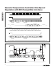
During a READ operation, the DOUT line goes low on
the falling clock edge after the READ/WRITE bit (8th
bit). The data in the shift register is moved to the DOUT
line during the 8th to 15th falling-clock edges and the
MSB of the data is available to be read at the rising
edge of the 9th clock pulse. The remaining clock puls-
es in the READ operation shift the register contents on
the negative clock edge so that they can be latched
into the master on the positive edge. Any READ opera-
tion with less than 16 bits results in truncated data.
Figure 3 shows the read cycle.
For a WRITE operation, the command byte is decoded
during the 8th clock pulse. Then data is loaded into the
shift register on the positive edges of the 9th to 16th
clock pulses and transferred to the appropriate register
on the negative edge of the 16th clock period. Any
WRITE operation that does not have the 16th clock
edge does not get shifted out of the shift register and
thus is ignored. Since returning CS high resets the SPI
interface at the end of a transfer, this cannot be done
until after the 16th falling clock edge. If CS is returned
high before this 16th falling clock edge, the appropriate
Remote Temperature-Controlled Fan-Speed
Regulator with SPI-Compatible Interface
8 _______________________________________________________________________________________
QSPI is a trademark of Motorola, Inc.
MICROWIRE is a trademark of National Semiconductor Corp.