
Manual


Detailed Description
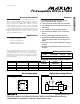
The MAX6900 contains eight timekeeping registers,
burst address registers, a control register, an on-chip
32.768kHz oscillator circuit, and a serial 2-wire, I
2
C-
compatible interface. There are also 31 bytes, 8 bits
wide of SRAM on board. Time and calendar data are
stored in the registers in a binary-coded decimal (BCD)
format. Figure 1 shows an I
2
C-bus-compatible timing
diagram. Figure 2 shows the MAX6900 functional dia-
gram.
Real-Time Clock
The RTC provides seconds, minutes, hours, day, date,
month, and year information. The end of the month is
automatically adjusted for months with fewer than 31
MAX6900
I
2
C-Compatible RTC in a TDFN
4 _______________________________________________________________________________________
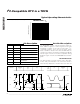
Typical Operating Characteristics
(T
A
= +25°C, unless otherwise noted.)
0
0.3
0.4
0.1
0.2
0.6
0.5
1.0
0.7
0.8
0.9
1.1
1.4
1.5
1.2
1.3
1.6
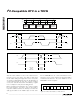
1.0 2.0 2.5 3.01.5 3.5 4.0 4.5 5.55.0 6.0
TIMEKEEPING CURRENT vs. V
CC
MAX6900 toc01
V
CC
(V)
TIMEKEEPING CURRENT (µA)
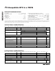
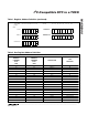
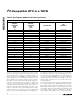
Pin Description
PIN NAME FUNCTION
1V
CC
Power Supply
2 X1 32.768kHz External Crystal
3 X2 32.768kHz External Crystal
4 GND Ground
5 SCL I
2
C-Bus-Compatible Clock Input
6 SDA
I
2
C-Bus-Compatible Data
Input/Output
— PAD Ground
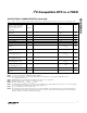
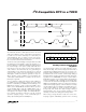
Figure 1. Detailed
I
2
C-Bus Timing Diagrams
PROTOCOL
START
CONDITION
(S)
ACKNOWLEDGE
(A)
STOP
CONDITION
(P)
BIT 7
MSB
(A7)
BIT 0
LSB
(R/W)
BIT 6
(A6)
SCL
t
SU:STA
t
HD:STA
t
HD:DAT
t
HD:DAT
t
SU:STO
1/f
SCL
t
HIGH
t
LOW
t
BUF
t
r
t
f
SDA