
User Manual


MAX7418–MAX7425
5th-Order, Lowpass,
Switched-Capacitor Filters
12 ______________________________________________________________________________________
and OS. Changing the voltage on COM or OS signifi-
cantly from midsupply reduces the dynamic range.
Power Supplies
The MAX7418–MAX7421 operate from a single +5V
supply and the MAX7422–MAX7425 operate from a sin-
gle +3V supply. Bypass V
DD
to GND with a 0.1µF
capacitor. If dual supplies are required, connect COM
to the system ground and GND to the negative supply.
Figure 5 shows an example of dual-supply operation.
Single-supply and dual-supply performance are equiv-
alent. For either single-supply or dual-supply operation,
drive CLK and SHDN from GND (V- in dual supply
operation) to V
DD
. Use the MAX7418–MAX7421 for
±2.5, and use the MAX7422–MAX7425 for ±1.5V. For
±5V dual-supply applications, refer to the MAX291/
MAX292/MAX295/MAX296 and MAX293/MAX294/
MAX297 data sheets.
Input Signal Amplitude Range
The optimal input signal range is determined by observ-
ing the voltage level at which the signal-to-noise plus
distortion (SINAD) ratio is maximized for a given corner
frequency. The Typical Operating Characteristics show
the THD + Noise response as the input signal’s peak-to-
peak amplitude is varied.
Anti-Aliasing and Post-DAC Filtering
When using the MAX7418–MAX7425 for anti-aliasing or
post-DAC filtering, synchronize the DAC (or ADC) and
the filter clocks. If the clocks are not synchronized, beat
frequencies may alias into the desired passband.
Harmonic Distortion
Harmonic distortion arises from nonlinearities within the
filter. These nonlinearities generate harmonics when a
pure sine wave is applied to the filter input. Tables 1, 2,
and 3 list typical harmonic distortion values with a 10kΩ
load at T
A
= +25°C.
Table 1. MAX7418/MAX7421/MAX7422/MAX7425 Typical Harmonic Distortion
FILTER
f
IN
(kHz)
V
IN
(Vp-p)
MAX7418
2
MAX7421
2
2
4
2nd 4th
f
CLK
(MHz)
2.2
1.5
2
<-80<-80
<-80
MAX7422
4
TYPICAL HARMONIC DISTORTION (dB)
<-80
<-80
4
2
2
4.0
2.2
<-80<-80
<-80
<-80
<-80
<-80
<-80
<-80
<-80
<-80 <-80
3rd 5th
2.2
1.5
<-80<-80
<-80
4
<-80
<-80
MAX7425
2
2
4.0
2.2
<-80
<-80
<-80
<-80
<-80
<-80
<-80
<-80
<-80
<-80
<-80
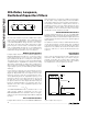
V
DD
V+
V-
IN
CLK
GND
INPUT
OUTPUTOUT
0.1
µ
F
CLOCK
*CONNECT SHDN TO V- FOR LOW-POWER SHUTDOWN MODE.
SHDN
COM
OS
0.1
µ
F
MAX7418–
MAX7425
*
V+
V-
Figure 5. Dual-Supply Operation