
User Manual
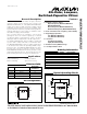

MAX7418–MAX7425
5th-Order, Lowpass,
Switched-Capacitor Filters
_______________________________________________________________________________________ 9
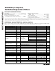
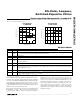
Pin Description
_______________Detailed Description
The MAX7418/MAX7421/MAX7422/MAX7425 elliptic
lowpass filters provide sharp rolloff with good stopband
rejection. The MAX7419/MAX7423 Bessel filters provide
low overshoot and fast settling responses, and the
MAX7420/MAX7424 Butterworth filters provide a maxi-
mally flat passband response. All parts operate with a
100:1 clock-to-corner frequency ratio.
Most switch capacitor filters (SCFs) are designed with
biquadratic sections. Each section implements two
pole-zero pairs, and the sections can be cascaded to
produce higher order filters. The advantage to this
approach is ease of design. However, this type of
design is highly sensitive to component variations if any
section’s Q is high. The MAX7418–MAX7425 use an
alternative approach, which is to emulate a passive net-
work using switched-capacitor integrators with sum-
ming and scaling. The passive network may be
synthesized using CAD programs, or may be found in
many filter books. Figure 1 shows a basic 5th-order lad-
der filter structure.
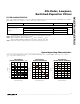
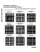
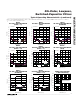
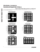
Typical Operating Characteristics (continued)
(V
DD
= +5V for MAX7418–MAX7421, V
DD
= +3V for MAX7422–MAX7425, f
CLK
= 2.2MHz, SHDN = V
DD
, V
COM
= V
OS
= V
DD
/ 2,
T
A
= +25°C, unless otherwise noted.
0
0.5
1.5
1.0
2.0
2.5
2.5 3.53.0 4.0 4.5 5.0 5.5
DC OFFSET VOLTAGE
vs. SUPPLY VOLTAGE
MAX7418 toc28
SUPPLY VOLTAGE (V)
DC OFFSET VOLTAGE (mV)
0
1.0
0.5
2.0
1.5
2.5
3.0
-40 10-15 356085
DC OFFSET VOLTAGE
vs. TEMPERATURE
MAX7418 toc27
TEMPERATURE (
°
C)
DC OFFSET VOLTAGE (mV)
V
DD
= 5V
V
DD
= 3V
Filter OutputOUT5
Offset Adjust Input. To adjust output offset, connect OS to an external supply through a resistive voltage-
divider (Figure 4). Connect OS to COM if no offset adjustment is needed. See the Offset and Common-Mode
Input Adjustment section.
OS6
Shutdown Input. Drive low to enable shutdown mode; drive high or connect to V
DD
for normal operation.
SHDN
7
Clock Input. Connect an external capacitor (C
OSC
) from CLK to ground. To override the internal oscillator,
connect CLK to an external clock: f
C
= f
CLK
/100.
CLK8
Positive Supply Input: +5V for MAX7418–MAX7421, +3V for MAX7422–MAX7425. Bypass V
DD
to GND with
a 0.1µF capacitor.
V
DD
4
Ground GND3
PIN
Filter InputIN2
Common Input Pin. Biased internally at midsupply. Bypass COM externally to GND with a 0.1µF capacitor.
To override internal biasing, drive COM with an external supply.
COM1
FUNCTIONNAME