
Instruction Manual

MAX7426/MAX7427
5th-Order, Lowpass, Elliptic,
Switched-Capacitor Filters
2 _______________________________________________________________________________________
ABSOLUTE MAXIMUM RATINGS
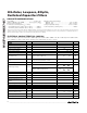
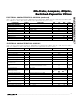
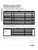
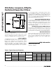
ELECTRICAL CHARACTERISTICS—MAX7426
(V
DD
= +5V, filter output measured at OUT, 10kΩ
|| 50pF load to GND at OUT, SHDN = V
DD
, OS = COM, 0.1µF from COM to GND,
f
CLK
= 100kHz, T
A
= T
MIN
to T
MAX
, unless otherwise noted. Typical values are at T
A
= +25°C.)
Stresses beyond those listed under “Absolute Maximum Ratings” may cause permanent damage to the device. These are stress ratings only, and functional
operation of the device at these or any other conditions beyond those indicated in the operational sections of the specifications is not implied. Exposure to
absolute maximum rating conditions for extended periods may affect device reliability.
V
DD
to GND..............................................................-0.3V to +6V
IN, OUT, COM, OS, CLK, SHDN ................-0.3V to (V
DD
+ 0.3V)
OUT Short-Circuit Duration.......................................................1s
Continuous Power Dissipation (T
A
= +70°C)
8-Pin µMAX (derate 4.1mW/°C above +70°C) .............330mW
8-Pin PDIP (derate 6.90mW/°C above +70°C).............552mW
Operating Temperature Ranges
MAX742 _C_A....................................................0°C to +70°C
MAX742 _E_A .................................................-40°C to +85°C
Storage Temperature Range .............................-65°C to +160°C
Lead Temperature (soldering, 10s) .................................+300°C
C
OSC
= 1000pF (Note 3)
V
OS
= 0 to V
DD
SHDN = GND, V
COM
= 0 to V
DD
(Note 1)
T
A
= +25°C
Input, COM externally driven
OS to OUT
Measured with respect to COM
f
IN
= 200Hz, V
IN
= 4Vp-p,
measurement bandwidth = 22kHz
V
IN
= V
COM
= V
DD
/ 2
V
COM
= V
DD
/ 2 (Note 2)
Output, COM internally driven
CONDITIONS
13.5 17.5 21.5f
OSC
Internal Oscillator Frequency
±0.2 ±10Input Leakage Current at OS
±0.2 ±10Input Leakage Current at COM
50 500C
L
10 1R
L
Resistive Output Load Drive
5Clock Feedthrough
90 130R
COM
Input Resistance at COM
±0.1V
OS
Input Voltage Range at OS
V
DD
- 0.2
V
DD
V
DD
+ 0.2
2 2 2
100:1f
CLK
/f
C
Clock-to-Corner Ratio
0.001 to 9f
C
Corner-Frequency Range
V
DD
- 0.5
V
DD
V
DD
+ 0.5
2 2 2
V
COM
COM Voltage Range
+1A
OS
Offset Voltage Gain
-81THD+N
Total Harmonic Distortion plus
Noise
10Clock-to-Corner Tempco
0.25 V
DD
- 0.25Output Voltage Range
±4 ±25V
OFFSET
Output Offset Voltage
0 0.2 0.4
DC Insertion Gain with Output
Offset Removed
MIN TYP MAXSYMBOLPARAMETER
0.5V
IL
Clock Input Low
4.5V
IH
Clock Input High
±8 ±12.5I
CLK
Clock Output Current
(internal oscillator mode)
V
V
µA
kHz
µA
µA
pF
kΩ
mVp-p
kΩ
V
V
V/V
dB
dB
mV
V
ppm/°C
kHz
UNITS
Maximum Capacitive Load
at OUT
FILTER
CLOCK