
Instruction Manual
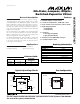

MAX7426/MAX7427
5th-Order, Lowpass, Elliptic,
Switched-Capacitor Filters
4 _______________________________________________________________________________________
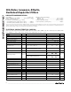
C
OSC
= 1000pF (Note 3)
CONDITIONS
13.5 17.5 21.5f
OSC
Internal Oscillator Frequency
MIN TYP MAXSYMBOLPARAMETER
Measured at DC
SHDN = GND
Operating mode, no load
V
CLK
= 0 or 3V
0.5V
SDL
SHDN Input Low
2.5V
SDH
SHDN Input High
70PSRRPower-Supply Rejection Ratio
0.2 1I
SHDN
Shutdown Current
0.75 1.0
2.7 3.6V
DD
Supply Voltage
0.5V
IL
Clock Input Low
2.5V
IH
Clock Input High
±7.5 ±12.5I
CLK
Clock Output Current
(internal oscillator mode)
V
V
dB
µA
V
V
V
µA
kHz
UNITS
SHDN Input Leakage Current
V
SHDN
= 0 to V
DD
±0.2 ±10 µA
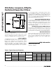
ELECTRICAL CHARACTERISTICS—MAX7427 (continued)
(V
DD
= +3V, filter output measured at OUT pin, 10kΩ
|| 50pF load to GND at OUT, SHDN = V
DD
, OS = COM, 0.1µF from COM to
GND, f
CLK
= 100kHz, T
A
= T
MIN
to T
MAX
, unless otherwise noted. Typical values are at T
A
= +25°C.)
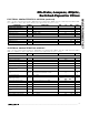
ELLIPTIC FILTER CHARACTERISTICS (r = 1.25)
(V
DD
= +5V for MAX7426, V
DD
= +3V for MAX7427, filter output measured at OUT, 10kΩ || 50pF load to GND at OUT, SHDN = V
DD,
V
COM
= V
OS
=V
DD
/ 2, f
CLK
= 100kHz, T
A
= T
MIN
to T
MAX
, unless otherwise noted. Typical values are at T
A
= +25°C.) (Note 3)
Note 1: The maximum f
C
is defined as the clock frequency f
CLK
= 100
✕
f
C
at which the peak SINAD drops to 68dB with a sinu-
soidal input at 0.2f
C
.
Note 2: DC insertion gain is defined as ∆V
OUT
/ ∆V
IN
.
Note 3: f
OSC
(kHz) ≈ 17.5
✕
10
3
/ C
OSC
(C
OSC
in pF).
Note 4: The input frequencies, f
IN
, are selected at the peaks and troughs of the ideal elliptic frequency responses.
f
IN
= 0.68f
C
f
IN
= 0.38f
C
f
IN
= 3.25f
C
f
IN
= 1.43f
C
f
IN
= 1.25f
C
f
IN
= 0.87f
C
f
IN
= 0.97f
C
f
IN
= f
C
CONDITIONS
-0.4 0.2 0.4
dB
-0.4 -0.2 0.4
Insertion Gain
with DC Gain Error Removed
(Note 4)
-37.2 -35
-37.2 -35
-38.5 -34
-0.4 -0.2 0.4
-0.4 0.2 0.4
-0.7 -0.2 0.2
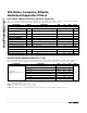
UNITSMIN TYP MAXPARAMETER
mAI
DD
Supply Current
CLOCK
POWER REQUIREMENTS
SHUTDOWN