
Instruction Manual

MAX7426/MAX7427
5th-Order, Lowpass, Elliptic,
Switched-Capacitor Filters
_______________________________________________________________________________________ 9
powered from 0 to V
DD
. Varying the rate of the external
clock adjusts the corner frequency of the filter:
Internal Clock
When using the internal oscillator, the capacitance
(C
OSC
) on CLK determines the oscillator frequency:
Since C
OSC
is in the low picofarads, minimize the stray
capacitance at CLK so that it does not affect the inter-
nal oscillator frequency. Varying the rate of the internal
oscillator adjusts the filter’s corner frequency by a
100:1 clock-to-corner frequency ratio. For example, an
internal oscillator frequency of 100kHz produces a
nominal corner frequency of 1kHz.
Input Impedance vs. Clock Frequencies
The MAX7426/MAX7427’s input impedance is effective-
ly that of a switched-capacitor resistor (see the following
equation), and is inversely proportional to frequency.
The input impedance values determined by the equa-
tion represent the average input impedance, since the
input current is not continuous. As a rule, use a driver
with an output resistance less than 10% of the filter’s
input impedance.
Estimate the input impedance of the filter by using the
following formula:
where f
CLK
= clock frequency and C
IN
= 1pF.
Low-Power Shutdown Mode
The MAX7426/MAX7427 have a shutdown mode that is
activated by driving SHDN low. In shutdown mode, the
filter supply current reduces to 0.2µA, and the output of
the filter becomes high impedance. For normal opera-
tion, drive SHDN high or connect to V
DD
.
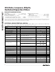
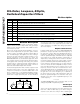
Applications Information
Offset (OS) and Common-Mode (COM)
Input Adjustment
COM sets the common-mode input voltage and is
biased at midsupply with an internal resistor-divider. If
the application does not require offset adjustment, con-
nect OS to COM. For applications where offset adjust-
ment is required, apply an external bias voltage
through a resistor-divider network to OS, as shown in
Figure 3. For applications that require DC level shifting,
adjust OS with respect to COM. (Note: Do not leave OS
unconnected.) The output voltage is represented by
these equations:
where (V
IN
- V
COM
) is lowpass filtered by the SCF and
OS is added at the output stage. See the Electrical
VVVV
V
V
typical
OUT IN COM OS
COM
DD
( )
()
=− +
=
2
Z
1
f C
IN
CLK IN
=
×
f (kHz)
17.5 10
C (pF)
OSC
3
OSC
=
×
f
f
C
CLK
=
100
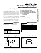
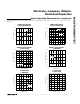
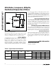
PASSBAND STOPBAND
GAIN (dB)
FREQUENCY
f
C
f
S
f
S
f
C
f
S
f
C
TRANSITION RATIO =
RIPPLE
V
DD
V
SUPPLY
IN
CLK
GND
INPUT
OUTPUT
50k
50k
50k
OUT
0.1µF
0.1µF
0.1µF
CLOCK
SHDN
COM
OS
MAX7426
MAX7427
Figure 2. Elliptic Filter Response
Figure 3. Offset Adjustment Circuit