
User Manual

MAX746
High-Efficiency, PWM, Step-Down,
N-Channel DC-DC Controller
______________________________________________________________________________________ 13
External Logic-Level N-FET Selection
To ensure the external N-FET is turned on hard, use
logic-level or low-threshold N-FETs. Three important
parameters to note when selecting the N-FET are the
total gate charge (Q
g
), on resistance (r
DS(ON)
), and
reverse transfer capacitance (C
RSS
).
Q
g
includes all capacitances associated with charging
the gate. Use the typical Q
g
value for best results; the
maximum value is usually grossly overspecified, since
it is a guaranteed limit and not the measured value.
The typical total gate charge should be 50nC or less;
with larger numbers, EXT may not be able to ade-
quately drive the gate. EXT sink/source capability
(I
EXT
) is typically 210mA.
The two most significant losses contributing to the
N-FET’s power dissipation are I
2
R losses and switching
losses. CCM power dissipation (P
D
), is approximated by:
P
D
= (Duty Cycle)(I
PK
2
)(r
DS(ON)
) +
(V+
2
)(C
RSS
)(I
PK
)(f
OSC
)
__________________________
(I
EXT
)
where the duty cycle is approximately V
OUT
/V+,
f
OSC
= 100kHz, and r
DS(ON)
and C
RSS
are given in the
data sheet of the chosen N-FET. In the equation,
r
DS(ON)
is assumed constant, but is actually a function
of temperature. The equation given does not account
for losses incurred by charging and discharging the
gate capacitance, because that energy is dissipated
by the gate-drive circuitry, not the N-FET.
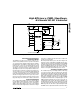
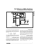
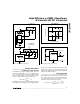
The Standard Application Circuits (Figure 1) use an
8-pin, Si9410DY, surface-mount N-FET that has 0.05Ω
on resistance with a 4.5V V
GS
. Optimum efficiency is
obtained when the voltage at the source swings between
the supply rails (within a few hundred millivolts).
Diode Selection
The MAX746’s high switching frequency demands a
high-speed rectifier. Schottky diodes are recommend-
ed. Ensure that the Schottky diode average current
rating exceeds the maximum load current.
Capacitor Selection
Output Filter Capacitor
The output filter capacitor C1 should have a low effec-
tive series resistance (ESR), and its capacitance should
remain fairly constant over temperature. This is espe-
cially true when in CCM, since the output filter capaci-
tor and the load form the dominant pole that
stabilizes the voltage loop.
To ensure stability, the minimum capacitance and max-
imum ESR values are:
(5)(V
REF
)
C1
(min)
>
______________________________
(2π)(GBW)(V
OUT
)(R
SENSE
)
and,
(V
OUT
)(R
SENSE
)
ESR
C1
<
___________________
(V
REF
)
where GBW = the loop gain-bandwidth product, 15kHz.
Sprague 595D surface-mount solid tantalum capacitors
and Sanyo OS-CON through-hole capacitors are rec-
ommended due to their extremely low ESR. OS-CON
capacitors are particularly useful at low temperatures.
For best results when using other capacitors, increase
the output filter capacitor’s size or use capacitors in
parallel to reduce the ESR.
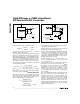
Bypass OUT with a 0.1µF (C4) capacitor to GND when using
a fixed 5V output (Figures 1a and 1c). With adjustable-output
operation, place C4 between the output voltage and AGND
as close to the IC as possible (Figure 1b).
The circuit load-step response is improved by using a
larger output filter capacitor or by placing a low-cost
bulk capacitor in parallel with the required low-ESR
output filter capacitor. The output voltage sag under a
load step (I
STEP
) is approximated by:
(I
STEP
2
)(L)
V
SAG
=
_____________________________________
(2)(C1)(V
IN(MIN
)(D
MAX
- V
OUT
)
where DMAX is the maximum duty cycle (91% worst
case). The equation assumes an input/output voltage
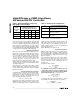
differential of 2V or more. Table 1 gives measured val-
ues of output voltage sag with a 30mA to 3A load step
for various input voltages and output filter capacitors.
Refer also to the
AC Stability with Low Input/Output
Differentials
section.
Input Bypass Capacitor
The input bypass capacitor C2 reduces peak currents
drawn from the voltage source, and also reduces the
amount of noise at the voltage source caused by the
MAX746’s fast switching action (this is especially
important when other circuitry is operated from the
same source). The input capacitor ripple current rating
must exceed the RMS input ripple current.
I
RMS
= RMS AC input current
√
(
V
OUT
)(
V
IN -
V
OUT
)
= I
LOAD
(
_______________________
)
V
IN