
User Manual

MAX746
High-Efficiency, PWM, Step-Down,
N-Channel DC-DC Controller
14 ______________________________________________________________________________________
For load currents up to 3A, 100µF (C2) in parallel with
0.1µF (C3) is adequate. Smaller bypass capacitors may
also be acceptable for lighter loads. The input voltage
source impedance determines the size of the capacitor
required at the V+ input. As with the output filter capaci-
tor, a low-ESR capacitor (Sanyo OS-CON, Sprague 595D
or equivalent) is recommended for input bypassing.
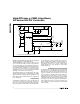
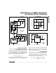
Charge-Pump Capacitors
Figure 3a shows the charge-pump doubler circuit con-
figured with a 0.1µF charge-pump capacitor C8 and a
1.0µF reservoir capacitor C9. The ratio of the capaci-
tors, along with the input voltage, determines the
amount of ripple on HIGH. If the input supply range
exceeds 12V, increase C9 to 4.7µF to reduce the
charge-pump ripple. C9 should be 10µF for less.
Figure 3b shows the charge-pump tripler circuit.
Refer to Table 2 to determine the proper charge-pump
configuration (which is based on the minimum expect-
ed supply voltage at V+).
Some interaction occurs between the switch oscillator
and the charge-pump oscillator. This interaction modu-
lates the inductor-current waveform, but has negligible
impact on the output.
Soft-Start and Reference Capacitors
Soft-start provides a ramp to the full current limit. A typi-
cal value for the soft-start capacitor (C5) is 0.1µF,
which provides a 380ms soft-start time. Use values in
the 0.001µF to 1µF range. The nominal time for C5 to
reach its steady-state value is given by:
t
SS
(sec) = (C5) (3.8 x 10
6
)
Note that t
SS
does NOT equal the time it takes for the
MAX746 to power-up, although it does affect the start-
up time. The start-up time is also a function of the input
voltage and load current. With a 3A load current, a 10V
input voltage, and a 0.1µF soft-start capacitor, it typi-
cally takes 240ms for the MAX746 to power up. A
0.47µF soft-start capacitor increases the start-up time
to approximately 2.3sec.
Bypass REF with a 1µF capacitor (C6).
Compensation Capacitor
With a fixed 5V output, connect a compensation capac-
itor (C7) between CC and AGND to optimize transient
response. Appropriate compensation is determined by
the size and ESR of the output filter capacitor (C1), and
by the load current.
In the standard 5V application circuit, 2.7nF is appro-
priate for load currents up to 3A; for lighter loads,
C7’s value can be reduced. If 2.7nF does not com-
pensate adequately, use the following equations to
determine C7.
For fixed 5V-output operation:
(
C1
)
(
ESR
C1
)
C7 =
_____________
12kΩ
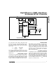
For adjustable-output operation, FB becomes the
compensation input pin, and CC and OUT are left
unconnected. Connect C7 between FB and GND in
parallel with R4 (Figure 6). C7 is determined by:
(2) (C1)(ESR
C1
)
C7 =
___________________
R4 R5
For example, with a fixed 5V output with C1 = 470µF
and an ESR
C1
of 0.04Ω (at a frequency of 100kHz):
(
C1
)(
ESR
C1
)
C7 =
_____________
= 1560pF
12kΩ
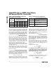
Table 1. Measured Output Voltage Sag
with 30mA to 3A Load Step*
Table 2. Charge-Pump Configuration
V+ CHARGE-PUMP CONFIGURATION
V+ ≤ 6V
6V < V+ < 6.5V*
V+ ≥ 6.5V*
Voltage tripler with 1N914 diodes for D2,
D3, D5, and D6
Voltage doubler with 1N5817 Schottky
diodes for D2 and D3
Voltage doubler with 1N914 diodes for
D2 and D3
* When using the voltage-doubler circuit over the military
temperature range, increase the 6.5V limit to 7V.
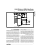
*Circuit of Figure 1a.
OUTPUT
FILTER
CAPACITOR
C1 ( F)
OUTPUT VOLTAGE SAG (mV)
FOR VARIOUS INPUT VOLTAGES
V
IN
=6V V
IN
=6.5V V
IN
=7V V
IN
=9V V
IN
=10V
440 400 250 210 140 90
660 260 190 160 70 50
880 200 100 90 40 25