
User Manual

MAX746
High-Efficiency, PWM, Step-Down,
N-Channel DC-DC Controller
______________________________________________________________________________________ 15
Increasing C7 by up to 50% enhances outer-loop
stability by adding stability to the inductor current
waveform. But increasing C7 too much causes
FB’s response time to decrease (due to the larger
RC time constant caused by the feedback resistors
and the compensation capacitor), which reduces
load-transient stability.
Setting the Low-Battery
Detector Voltage
Select R1 between 10kΩ and 1MΩ. Determine R2 using
the following equation:
(V
TRIP
- V
REF
)
R2 = R1
(
________________
)
V
REF
where V
REF
is typically 2.0V. Connect a pull-up resistor
(e.g., 100kΩ) between LBO and V
OUT
(Figure 5).
Using a Second Supply in
Place of the Charge Pump
If a secondary power supply (a minimum of 5V above
the main supply) is available, it can be substituted for
the charge-pump high-side supply. In this case,
bypass HIGH with a 1µF capacitor and leave CP
unconnected. Since this secondary supply voltage
is applied to the gate, V
GS
must not exceed the
gate-source breakdown voltage of the external N-FET.
Also, the voltage at HIGH must not exceed 20V. If
a secondary supply is used, the shutdown function
cannot be used because HIGH is internally tied to
V+ in shutdown mode. In this case, SHDN must be
tied low. With the main supply off and HIGH at 12V,
HIGH will typically sink 130µA.
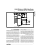
Layout Considerations
Because high current levels and fast switching wave-
forms radiate noise, proper PC board layout is essen-
tial. Use a ground plane, and minimize ground noise by
connecting GND, the anode of the steering Schottky
diode, the input bypass-capacitor ground lead, and the
output filter capacitor ground lead to a single point (star
ground configuration). Also minimize lead lengths to
reduce stray capacitance, trace resistance, and radiat-
ed noise. Place bypass capacitor C3 as close to V+
and GND as possible.
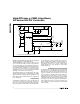
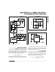
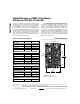
AV+ and CS are the inputs to the differential-input
current-sense amplifier. Use a Kelvin connection
across the sense resistor, as shown in Figure 8.
Although AV+ also functions as the supply voltage
for sensitive analog circuitry, a separate AV+ bypass
capacitor should not be used. By not using a capaci-
tor, any noise at the CS input will also appear at the
AV+ input, and will be interpreted by the current-
sense amplifier as a common-mode signal . A sepa-
rate AV+ capacitor causes the noise to appear on
only one input, and this differential noise will be
amplified, adversely affecting circuit operation.
Additional Notes
When probing the MAX746 circuit, avoid shorting
V+ to GND (the two pins are adjacent) as this may
cause the IC to malfunction because of large ground
currents. Because of its fast switching and high drive-
capability requirements, EXT is a low-impedance point
that is not short-circuit protected. Therefore, do not
short EXT to any node (including AGND and V+, which
are adjacent to EXT).
Similarly, CC (or FB in adjustable-output operation) is a
sensitive input that should not be shorted to any node.
Avoid shorting CC when probing the circuit, as this may
damage the device.
The MAX746 may continue to operate with AV+ discon-
nected, but erratic switching waveforms will appear at EXT.
Switching Waveforms
There is a region between CCM and DCM where the
inductor current operates in both modes, as shown
in the Idle-Mode Moderate Current EXT waveform in
the
Typical Operating Characteristics
. As the out-
put voltage varies, it is fed back into CC and the
duty cycle adjusts to compensate for this change.
The switch is considered off when V
EXT
is less than
AV+
V
IN
CS
R
SENSE
N
EXT
L1
V
OUT
KELVIN SENSE
CONNECTION
V+
MAX746
Figure 8. Kelvin Connection for Current-Sense Amplifier