
User Manual

Maxim cannot assume responsibility for use of any circuitry other than circuitry entirely embodied in a Maxim product. No circuit patent licenses are
implied. Maxim reserves the right to change the circuitry and specifications without notice at any time.
16
__________________Maxim Integrated Products, 120 San Gabriel Drive, Sunnyvale, CA 94086 (408) 737-7600
© 1993 Maxim Integrated Products Printed USA is a registered trademark of Maxim Integrated Products.
MAX746
High-Efficiency, PWM, Step-Down,
N-Channel DC-DC Controller
SUPPLIER PHONE FAX
Coiltronics (305) 781-8900 (305) 782-4163
Gowanda (716) 532-2234 (716) 532-2702
Sumida USA (708) 956-0666 (708) 956-0702
Sumida Japan 81-3-3607-511 81-3-3607-5428
Kemet (803) 963-6300 (803) 963-6322
Matsuo (714) 969-2491 (714) 960-6492
Nichicon (708) 843-7500 (708) 843-2798
Sprague (603) 224-1961 (603) 224-1430
Sanyo Japan 81-3-3837-6242
United Chemi-Con (714) 255-9500 (714) 255-9400
Motorola (800) 521-6274
Nihon USA (805) 867-2555 (805) 867-2698
Nihon Japan 81-3-3494-7411 81-3-3494-7414
Harris (407) 724-3739 (407) 724-3937
International Rectifier (213) 772-2000 (213) 772-9028
Siliconix (408) 988-8000 (408) 727-5414
IRC (512) 992-7900 (512) 992-3377
Sanyo USA (619) 661-6322
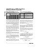
INDUCTORS
CAPACITORS
DIODES
POWER TRANSISTORS
RESISTORS
Table 3. Component Suppliers
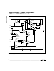
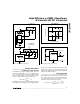
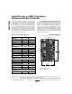
___________________Chip Topography
or equal to the N-FET’s V
GS
threshold voltage. Once
the switch is off, the voltage at EXT is pulled to GND
and the N-FET source voltage is a Schottky diode
drop below GND. However, this is not always the case
in the “in-between” mode, due to the changing duty
cycle inherent with DCM. When the device is at maxi-
mum duty cycle, EXT turns off at V
GS
, but the switch
sometimes turns on again after the minimum off-time
before EXT can be pulled to GND. This results in short
spikes, which can be seen on the EXT waveform in the
Typical Operating Characteristics
.
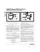
AC Stability with Low Input/Output Differentials
At low input/output differentials, the inductor current
cannot slew quickly enough to respond to load
changes, so the output filter capacitor must hold up the
voltage as the load transient is applied. In Figure 1a’s
circuit, for V+ = 6V, increase the output filter capacitor
to 900µF (Sprague 595D low-ESR capacitors) to obtain
a transient response less than 250mV with a load step
from 0.1A to 3A. As V+ increases, the inductor current
slews faster, so the size of the output filter capacitor can
be reduced (see Table 1).
HIGH
AGND
EXT
SS
REF
SHDN
LBI
LBO GND
CS
OUT CC
FB
AV+
0.130"
(3.30mm)
0.080"
(2.03mm)
TRANSISTOR COUNT: 508;
SUBSTRATE CONNECTED TO HIGH.
V+
CP