
User Manual

MAX746
High-Efficiency, PWM, Step-Down,
N-Channel DC-DC Controller
6 _______________________________________________________________________________________
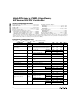
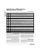
______________________________________________________________Pin Description
PIN NAME FUNCTION
1 LBO
3 SS
4 REF
5 SHDN
6 FB
7 CC
8 AV+
9 OUT
10 CS
11 AGND Quiet analog ground.
12 EXT
13 HIGH Regulated high-side voltage, 5V above the V+ supply voltage.
14 CP Charge-pump output that generates a 0V to V+, 50kHz square wave (see
Charge Pump
section).
15 V+ High-current supply voltage for the charge pump.
Low-battery output is an open-drain output that goes low when LBI is less than 2V. Connect to V+ through a
pull-up resistor. Leave floating if not used. LBO is disabled in shutdown mode.
Soft-start limits start-up surge currents. On power-up, it charges the soft-start capacitor, slowly raising the peak
current limit to the level set by the sense resistor.
2V reference output can source 100µA for external loads. Bypass with 1µF. The reference is disabled in shutdown mode.
Active-high logic input. In shutdown mode, V
OUT
= 0V and the supply current is reduced to less than 20µA.
Connect to GND for normal operation.
Feedback input for adjustable-output operation. Connect to GND for fixed 5V output. Use a resistor-divider net-
work to adjust the output voltage (see
Setting the Output Voltage
section).
AC compensation input for the error amplifier. Connect a capacitor between CC and GND for fixed 5V-output
operation (see
Compensation Capacitor
section).
Quiet supply voltage for sensitive analog circuitry. Also the noninverting input to the current-sense amplifier. A
separate bypass capacitor is not recommended for AV+.
Output voltage sense that connects to the internal resistor divider. Bypass with 0.1µF to AGND, close to the IC
for fixed output operation. Leave unconnected for adjustable-output operation.
Inverting input to the current-sense amplifier. Connect the current-sense resistor (R
SENSE
) from AV+ to CS.
Power MOSFET gate-drive output that swings between HIGH and GND. EXT is not protected against short cir-
cuits to V+ or AGND.
16 GND High-current ground return for the output driver and charge pump.
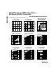
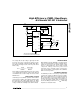
____________________Getting Started
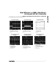
Figure 1a shows the 5V-output 3A standard application
circuit, Figure 1b shows the 3.3V-output 3A standard
application circuit, and Figure 1c shows the 5V-output
1.5A standard application circuit. Most applications will
be served by these circuits. To learn more about compo-
nent selection for particular applications, refer to the
Design Procedure
section. To learn more about the oper-
ation of the MAX746, refer to the
Detailed Description
.
_______________Detailed Description
The MAX746 monolithic, CMOS, step-down, switch-
mode power-supply controller provides high-side drive
for external logic-level N-channel FETs. A charge pump
generates a voltage 5V above the supply voltage for
high-side drive capability. The MAX746 uses a unique
current-mode pulse-width-modulating (PWM) control
scheme that results in tight output-voltage regulation,
excellent load- and line-transient response, low noise,
and high efficiency over a wide range of load currents.
Efficiency at light loads is further enhanced by a propri-
etary idle-mode switching control scheme that skips
oscillator cycles in order to reduce switching losses.
Other features include undervoltage lockout, shutdown,
and a low-battery detection comparator.
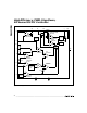
Operating Principle
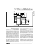
Figure 2 is the MAX746 block diagram. The MAX746
regulates using an inner current-feedback loop and an
outer voltage-feedback loop. A slope-compensation
scheme stabilizes the current loop; the dominant pole,
formed by the output filter capacitor and the load,
stabilizes the voltage loop.
2 LBI Input to the low-battery comparator. Tie to V+ or GND if not used.