
User Manual

MAX7461
General Description
The MAX7461 single-channel LOS alarm is ideal for any
video system needing to verify the presence of a video
source. The device accepts an AC-coupled CVBS, Y,
or any video signal with sync, and pulls LOS low when
no composite sync signal is detected for more than the
LOS detect time (3.4ms, typ) at the input (IN).
Clamp
The MAX7461 features an input clamp that corrects any
DC shift, on a line-by-line basis. The external AC-cou-
pling capacitor provides DC isolation for the input.
Lowpass Filter
The MAX7461 integrates a lowpass filter for enhanced
sync detection. The lowpass filter prevents false sync
detection by reducing color burst, chroma, and noise.
Sync Detector/LOS Filter
The sync detector looks for sync pulses greater than
the minimum sync voltage (0.13V
P-P
). If the detector
does not detect any sync pulses for 3.4ms (typ), the
LOS filter pulls LOS low. After detecting sync for at
least 2.2ms (typ), the LOS filter returns LOS to a high-
impedance state. LOS is an open-drain output.
Connect a 1kΩ pullup resistor between LOS and V
CC
.
Power-On Reset (POR)
At power-up, LOS is pulled low and the MAX7461
checks for 2.2ms (typ) of valid sync pulses before
releasing LOS. LOS remains high impedance while a
valid sync signal is detected at the input.
Applications Information
Input Considerations
Use 0.1µF ceramic capacitors to AC-couple the input.
The input cannot be DC-coupled. The input capacitor
stores a DC level so that the video signal is clamped to
an appropriate DC voltage for proper sync detection.
Power-Supply Bypassing
Careful PC board layout is important for optimal system
performance. Do not use wire-wrapped boards or
breadboards. When possible, use a multilayer board
with a dedicated low-inductance ground plane and
supply plane. Connect all GND inputs to a single
ground plane and V
CC
to a single-supply plane.
Bypass V
CC
to GND with a 0.1µF capacitor.
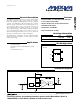
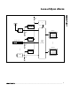
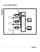
Wired-OR Application
The LOS open-drain output allows the MAX7461 to be
used in wired-OR applications as shown in the automo-
tive RSE typical application diagram of Figure 1.
Chip Information
PROCESS: BiCMOS
Loss-of-Sync Alarm
4 _______________________________________________________________________________________
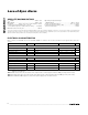
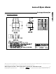
Pin Description
PIN NAME FUNCTION
1IN
Video Input. Accepts CVBS, luma (Y), or any video input with sync. AC-couple IN with a series 0.1µF
capacitor.
2, 3 GND Ground
4 LOS
Loss-Of-Sync Output (Open Drain). LOS is in high impedance when sync pulses are detected, and is
pulled low when no horizontal sync signal is detected for more than the LOS detect time. LOS returns
high when sync pulses are detected for more than the LOS release time. Connect a 1kΩ pullup resistor
from LOS to V
CC
.
5V
CC
Power-Supply Input. Bypass to GND with a 0.1µF capacitor.