
Manual
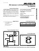

MAX834/MAX835
Micropower, Latching Voltage Monitors
in SOT23-5
6 _______________________________________________________________________________________
_______________Detailed Description
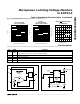
The MAX834/MAX835 micropower voltage monitors con-
tain a 1.204V precision bandgap reference and a com-
parator with an output latch (Figure 1). The difference
between the two parts is the structure of the comparator
output driver. The MAX834 has an open-drain, N-channel
output driver that can be pulled up to a voltage higher
than V
CC
, but less than 11V. The MAX835’s output is
push/pull and can both source and sink current.
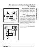
Programming the Trip Voltage (V
TRIP
)
Two external resistors set the trip voltage, V
TRIP
(Figure
2). V
TRIP
is the point at which the falling monitored volt-
age (typically V
CC
) causes OUT to go low. IN’s high
input impedance allows the use of large-value
resistors without compromising trip voltage accuracy. To
minimize current consumption, choose a value for R2
between 500kΩ and 1MΩ, then calculate R1 as follows:
R1 = R2 [(V
TRIP
/ V
TH
) - 1]
where V
TRIP
is the desired trip voltage and V
TH
is the
threshold voltage (1.204V). The voltage at IN must be at
least 1V less than V
CC
.
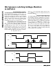
Latched-Output Operation
The MAX834/MAX835 feature a level-sensitive latch
input (CLEAR), designed to eliminate the need for hys-
teresis in battery undervoltage-detection applications.
When the monitored voltage (V
MON
) is above the pro-
grammed trip voltage (V
TRIP
) (as when the system bat-
tery is recharged or a fresh battery is installed), pulse
CLEAR low-high-low for at least 1µs to reset the output
latch (OUT goes high). When V
MON
falls below V
TRIP
,
OUT goes low and remains low (even if V
MON
rises
above V
TRIP
), until CLEAR is pulsed high again with
V
MON
> V
TRIP
. Figure 3 shows the timing relationship
between V
MON
, OUT, and CLEAR.
> 1µs
> 1µs
> V
TRIP
< V
TRIP
V
CC
CLEAR
V
CC
0V
0V
OUT
> 1µs
V
MON
> V
TRIP
< V
TRIP
V
CC
0V
OUT
V
MON
Figure 3a. Timing Diagram
Figure 3b. Timing Diagram, CLEAR = V
CC