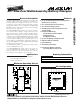
9-2764; Rev 1; 1/04 KIT ATION EVALU LE B A IL A AV Low-Cost Multichemistry Battery Chargers Features The MAX1908/MAX8724 highly integrated, multichemistry battery-charger control ICs simplify the construction of accurate and efficient chargers. These devices use analog inputs to control charge current and voltage, and can be programmed by the host or hardwired. The MAX1908/ MAX8724 achieve high efficiency using a buck topology with synchronous rectification.
MAX1908/MAX8724 Low-Cost Multichemistry Battery Chargers ABSOLUTE MAXIMUM RATINGS DCIN, CSSP, CSSN, ACOK to GND.......................-0.3V to +30V BST to GND ............................................................-0.3V to +36V BST to LX..................................................................-0.3V to +6V DHI to LX ...................................................-0.3V to (VBST + 0.3V) LX to GND .................................................................
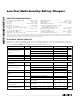
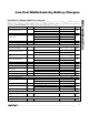
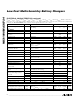
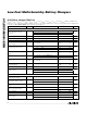
Low-Cost Multichemistry Battery Chargers (VDCIN = VCSSP = VCSSN = 18V, VBATT = VCSIP = VCSIN = 12V, VREFIN = 3V, VVCTL = VICTL = 0.75 x VREFIN, CELLS = float, CLS = REF, VBST - VLX = 4.5V, ACIN = GND = PGND = 0, CLDO = 1µF, LDO = DLOV, CREF = 1µF; CCI, CCS, and CCV are compensated per Figure 1a; TA = 0°C to +85°C, unless otherwise noted. Typical values are at TA = +25°C.
MAX1908/MAX8724 Low-Cost Multichemistry Battery Chargers ELECTRICAL CHARACTERISTICS (continued) (VDCIN = VCSSP = VCSSN = 18V, VBATT = VCSIP = VCSIN = 12V, VREFIN = 3V, VVCTL = VICTL = 0.75 x VREFIN, CELLS = float, CLS = REF, VBST - VLX = 4.5V, ACIN = GND = PGND = 0, CLDO = 1µF, LDO = DLOV, CREF = 1µF; CCI, CCS, and CCV are compensated per Figure 1a; TA = 0°C to +85°C, unless otherwise noted. Typical values are at TA = +25°C.
Low-Cost Multichemistry Battery Chargers (VDCIN = VCSSP = VCSSN = 18V, VBATT = VCSIP = VCSIN = 12V, VREFIN = 3V, VVCTL = VICTL = 0.75 x VREFIN, CELLS = float, CLS = REF, VBST - VLX = 4.5V, ACIN = GND = PGND = 0, CLDO = 1µF, LDO = DLOV, CREF = 1µF; CCI, CCS, and CCV are compensated per Figure 1a; TA = 0°C to +85°C, unless otherwise noted. Typical values are at TA = +25°C.
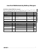
MAX1908/MAX8724 Low-Cost Multichemistry Battery Chargers ELECTRICAL CHARACTERISTICS (VDCIN = VCSSP = VCSSN = 18V, VBATT = VCSIP = VCSIN = 12V, VREFIN = 3V, VVCTL = VICTL = 0.75 x VREFIN, CELLS = FLOAT, CLS = REF, VBST - VLX = 4.5V, ACIN = GND = PGND = 0, CLDO = 1µF, LDO = DLOV, CREF = 1µF; CCI, CCS, and CCV are compensated per Figure 1a; TA = -40°C to +85°C, unless otherwise noted.
Low-Cost Multichemistry Battery Chargers (VDCIN = VCSSP = VCSSN = 18V, VBATT = VCSIP = VCSIN = 12V, VREFIN = 3V, VVCTL = VICTL = 0.75 x VREFIN, CELLS = FLOAT, CLS = REF, VBST - VLX = 4.5V, ACIN = GND = PGND = 0, CLDO = 1µF, LDO = DLOV, CREF = 1µF; CCI, CCS, and CCV are compensated per Figure 1a; TA = -40°C to +85°C, unless otherwise noted.
MAX1908/MAX8724 Low-Cost Multichemistry Battery Chargers ELECTRICAL CHARACTERISTICS (continued) (VDCIN = VCSSP = VCSSN = 18V, VBATT = VCSIP = VCSIN = 12V, VREFIN = 3V, VVCTL = VICTL = 0.75 x VREFIN, CELLS = FLOAT, CLS = REF, VBST - VLX = 4.5V, ACIN = GND = PGND = 0, CLDO = 1µF, LDO = DLOV, CREF = 1µF; CCI, CCS, and CCV are compensated per Figure 1a; TA = -40°C to +85°C, unless otherwise noted.) (Note 2) PARAMETER SYMBOL CELLS Input Float Voltage CONDITIONS MIN TYP (VREFIN / 2) 0.
Low-Cost Multichemistry Battery Chargers LDO LOAD REGULATION MAX1908 toc04 LDO LINE REGULATION VDCIN 10V/div -0.1 -0.2 INDUCTOR CURRENT 500mA/div -0.3 -0.4 -0.5 -0.6 0.03 0.01 0 -0.02 -0.8 -0.03 VLDO = 5.4V -0.9 -0.04 -1.0 -0.05 0 1 2 3 4 5 6 7 8 9 10 8 0.08 0.06 -0.04 -0.05 -0.06 0.04 90 80 EFFICIENCY (%) VREF ERROR (%) VREF ERROR (%) -0.03 100 MAX1908 toc08 0.02 0 -0.02 60 -0.04 30 -0.06 20 -0.09 -0.08 10 -0.10 -0.
Typical Operating Characteristics (continued) (Circuit of Figure 1, VDCIN = 20V, TA = +25°C, unless otherwise noted.) ICHG ERROR vs. CHARGE CURRENT CURRENT SETTING ERROR vs. ICTL 4 MAX1908 toc14 5.0 MAX1908 toc13 4.5 4.0 VREFIN = 3.3V VREFIN = 3.3V 3.5 3 ICHG (%) CURRENT-SETTING ERROR (%) 5 2 1 3.0 VBATT = 16V VBATT = 12V VBATT = 8V 2.5 2.0 1.5 1.0 0 0.5 0 -1 0 0.5 1.0 1.5 0 2.0 0.5 1.0 IINP ERROR vs. SYSTEM LOAD CURRENT 2.0 2.5 3.0 IINP ERROR vs.
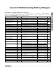
Low-Cost Multichemistry Battery Chargers PIN NAME 1 DCIN Charging Voltage Input. Bypass DCIN with a 1µF capacitor to PGND. FUNCTION 2 LDO Device Power Supply. Output of the 5.4V linear regulator supplied from DCIN. Bypass with a 1µF capacitor to GND. 3 CLS Source Current-Limit Input. Voltage input for setting the current limit of the input source. 4 REF 4.096V Voltage Reference. Bypass REF with a 1µF capacitor to GND. 5 CCS Input-Current Regulation Loop-Compensation Point. Connect a 0.
MAX1908/MAX8724 Low-Cost Multichemistry Battery Chargers Detailed Description The MAX1908/MAX8724 include all the functions necessary to charge Li+ batteries. A high-efficiency synchronous-rectified step-down DC-DC converter controls charging voltage and current. The device also includes input source current limiting and analog inputs for setting the charge current and charge voltage. Control charge current and voltage using the ICTL and VCTL inputs, respectively.
Low-Cost Multichemistry Battery Chargers AC ADAPTER INPUT 8.5V TO 28V RS1 0.01Ω D1 0.1µF D2 R6 59kΩ 1% R7 19.6kΩ 1% TO EXTERNAL LOAD CSSP CSSN CELLS DCIN C5 1µF C1 2 × 10µF 0.1µF (FLOAT-THREE CELLS SELECT) LDO LDO C13 1µF VCTL R13 33Ω D3 BST D/A OUTPUT ICTL DLOV 12.6V OUTPUT VOLTAGE VCC C15 0.1µF REFIN R8 1MΩ ACIN LX SHDN OUTPUT N1a DHI ACOK C16 1µF N1b DLO MAX1908 MAX8724 ICHG A/D INPUT L1 10µH PGND IINP A/D INPUT CCV C14 0.1µF R9 20kΩ C20 0.
Low-Cost Multichemistry Battery Chargers MAX1908/MAX8724 Typical Application Circuits (continued) AC ADAPTER INPUT 8.5V TO 28V RS1 0.01Ω P1 TO EXTERNAL LOAD R11 15kΩ C1 2 × 10µF 0.01µF 0.01µF R12 12kΩ LDO R6 59kΩ 1% CSSP ACOK DCIN D2 R7 19.6kΩ 1% CSSN CELLS C5 1µF R14 10.5kΩ 1% LDO VCTL LDO C13 1µF R13 33Ω D3 REFIN BST R15 8.25kΩ 1% DLOV 16.8V OUTPUT VOLTAGE 2.5A CHARGE LIMIT R16 8.25kΩ 1% FROM HOST µP (SHUTDOWN) REFIN (4 CELLS SELECT) N C15 0.
Low-Cost Multichemistry Battery Chargers MAX1908 MAX8724 DCIN SHDN 23.5% REFIN LDO RDY GND LOGIC BLOCK 5.4V LINEAR REGULATOR 4.096V REFERENCE REF GND 1/55 REFIN ICTL SRDY ACIN ACOK DCIN N REF/2 CCS CLS X CSSP 75mV REF CSIP GM ICHG CSI LEVEL SHIFTER CSIN IINP GMS LEVEL SHIFTER CSSN GM BST ICTL X GMI 75mV REFIN LEVEL SHIFTER DRIVER DHI CCI MAX1908 ONLY 3.
MAX1908/MAX8724 Low-Cost Multichemistry Battery Chargers Setting the Charging-Current Limit The ICTL input sets the maximum charging current. The current is set by current-sense resistor RS2, connected between CSIP and CSIN. The full-scale differential voltage between CSIP and CSIN is 75mV; thus, for a 0.015Ω sense resistor, the maximum charging current is 5A. Battery-charging current is programmed with ICTL using the equation: ICHG = VICTL 0.
Low-Cost Multichemistry Battery Chargers LDO Regulator LDO provides a 5.4V supply derived from DCIN and can deliver up to 10mA of load current. The MOSFET drivers are powered by DLOV and BST, which must be connected to LDO as shown in Figure 1. LDO supplies the 4.096V reference (REF) and most of the control circuitry. Bypass LDO with a 1µF capacitor to GND. Shutdown The MAX1908/MAX8724 feature a low-power shutdown mode. Driving SHDN low shuts down the MAX1908/ MAX8724.
Low-Cost Multichemistry Battery Chargers MAX1908/MAX8724 DC-DC Functional Diagram 5ms S RESET CSSP BST IMAX R 1.8V CSS X20 MAX1908 MAX8724 Q R AC ADAPTER RS1 D3 BST Q N1a DHI DHI CCMP LDO CSSN CBST LX CHG S IMIN Q 0.15V DLO N1b DLO L1 tOFF GENERATOR CSIP ZCMP 0.1V CSI X20 LVC RS2 CSIN GMS BATT COUT BATTERY GMI GMV SETV CONTROL SETI CLS CELLS CCS CCI CELL SELECT LOGIC CCV Figure 4.
Low-Cost Multichemistry Battery Chargers V − VBATT t OFF = 2.5µs × DCIN VDCIN t ON = L × IRIPPLE VCSSN − VBATT where: V ×t IRIPPLE = BATT OFF L f= 1 t ON + t OFF These equations result in fixed-frequency operation over the most common operating conditions. At the end of the fixed off-time, another cycle begins if the control point (LVC) is greater than 0.15V, IMIN = high, and the peak charge current is less than 6A (RS2 = 0.015Ω), IMAX = high.
MAX1908/MAX8724 Low-Cost Multichemistry Battery Chargers where RL varies with load according to RL = VBATT / ICHG.
Low-Cost Multichemistry Battery Chargers fP _ OUT = 1 = 1.08kHz 2πRL × COUT where: RL = ∆VBATT = Battery ESR ∆ICHG Set the compensation zero (fZ_CV) such that it is equivalent to the output pole (fP_OUT = 1.08kHz), effectively producing a pole-zero cancellation and maintaining a single-pole system response: fZ _ CV = 1 2πRCV × CCV CCI Loop Definitions Compensation of the CCI loop depends on the parameters and components shown in Figure 7. CCI is the CCI loop compensation capacitor.
CSIP To calculate the CCI loop compensation pole, CCI: GMI = 1µA/mV GMOUT = 3.33A/V ROGMI = 10MΩ f = 400kHz Choose crossover frequency f CO_CI to be 1/5th the MAX1908/MAX8724 switching frequency: CSIN GMOUT RS2 CSI CCI ROGMI CCI GMI = 80kHz 2πCCI fCO _ CI = GMI Solving for CCI, CCI = 2nF. To be conservative, set CCI = 10nF, which sets the crossover frequency at: ICTL fCO _ CI = Figure 7.
Low-Cost Multichemistry Battery Chargers fP _ CS = CSSP MAX1908/MAX8724 the charge-current amplifier transconductance = 1µA/mV. GM IN is the DC-DC converter transconductance = 3.3A/V.
Choose crossover frequency fCO_CS to be 1/5th the MAX1908/MAX8724 switching frequency: fCO _ CS = GMS = 80kHz 2πCCS where: tOFF = 2.5µs × (VDCIN – VBATT) / VDCIN VBATT < 0.88 × VDCIN or: tOFF = 0.3µs Solving for CCS, CCS = 2nF. To be conservative, set CCS = 10nF, which sets the crossover frequency at: fCO _ CS = GMS = 16kHz 2π10nF The compensation pole, fP_CS is set at: fP _ CS = 1 = 0.
Low-Cost Multichemistry Battery Chargers I 2.5µs C1 > C1 × 2 0.5V Both tantalum and ceramic capacitors are suitable in most applications. For equivalent size and voltage rating, tantalum capacitors have higher capacitance, but also higher ESR than ceramic capacitors. This makes it more critical to consider ripple current and power-dissipation ratings when using tantalum capacitors. A single ceramic capacitor often can replace two tantalum capacitors in parallel.
MAX1908/MAX8724 Low-Cost Multichemistry Battery Chargers 2) Place the IC and signal components. Keep the main switching node (LX node) away from sensitive analog components (current-sense traces and REF capacitor). Important: The IC must be no further than 10mm from the current-sense resistors. Keep the gate-drive traces (DHI, DLO, and BST) shorter than 20mm, and route them away from the current-sense lines and REF. Place ceramic bypass capacitors close to the IC.
Low-Cost Multichemistry Battery Chargers b CL D/2 PIN # 1 I.D. QFN THIN.EPS D2 0.15 C A D 0.10 M C A B D2/2 k 0.15 C B PIN # 1 I.D. 0.35x45∞ E/2 E2/2 CL (NE-1) X e E E2 k L DETAIL A e (ND-1) X e CL CL L L e e 0.10 C A C 0.08 C A1 A3 PROPRIETARY INFORMATION TITLE: PACKAGE OUTLINE 16, 20, 28, 32L, QFN THIN, 5x5x0.8 mm APPROVAL COMMON DIMENSIONS DOCUMENT CONTROL NO. REV. 21-0140 C 1 2 EXPOSED PAD VARIATIONS NOTES: 1. DIMENSIONING & TOLERANCING CONFORM TO ASME Y14.5M-1994.