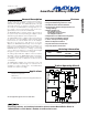
9-3885; Rev 0; 12/05 KIT ATION EVALU LE B A IL A AV Low-Cost Battery Charger The MAX8730 highly integrated, multichemistry, batterycharger control IC simplifies construction of accurate and efficient chargers. The MAX8730 operates at high switching frequency to minimize external component size and cost. The MAX8730 uses analog inputs to control charge current and voltage, and can be programmed by a microcontroller or hardwired.
MAX8730 Low-Cost Battery Charger ABSOLUTE MAXIMUM RATINGS CSSP, SRC, ACOK, ASNS, DHIV, BATT, CSIP to GND.......................................................-0.3V to +30V CSIP to CSIN or CSSP to CSSN ............................-0.3V to +0.3V DHIV to SRC .................................................-6V to (SRC + 0.3V) DHI to DHIV ...............................................-0.3V to (SRC + 0.3V) PDL, PDS to GND ........................................-0.3V to (SRC + 0.
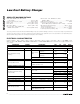
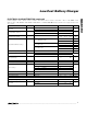
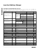
Low-Cost Battery Charger (Circuit of Figure 1. VSRC = VASNS = VCSSP = VCSSN = 18V, VBATT = VCSIP = VCSIN = 12V, VVCTL = VICTL = 1.8V, MODE = float, ACIN = 0, CLS = REF, REFON = LDO, INPON = LDO, RELTH = 2V. TA = 0°C to +85°C, unless otherwise noted. Typical values are at TA = +25°C.
MAX8730 Low-Cost Battery Charger ELECTRICAL CHARACTERISTICS (continued) (Circuit of Figure 1. VSRC = VASNS = VCSSP = VCSSN = 18V, VBATT = VCSIP = VCSIN = 12V, VVCTL = VICTL = 1.8V, MODE = float, ACIN = 0, CLS = REF, REFON = LDO, INPON = LDO, RELTH = 2V. TA = 0°C to +85°C, unless otherwise noted. Typical values are at TA = +25°C.
Low-Cost Battery Charger (Circuit of Figure 1. VSRC = VASNS = VCSSP = VCSSN = 18V, VBATT = VCSIP = VCSIN = 12V, VVCTL = VICTL = 1.8V, MODE = float, ACIN = 0, CLS = REF, REFON = LDO, INPON = LDO, RELTH = 2V. TA = 0°C to +85°C, unless otherwise noted. Typical values are at TA = +25°C.) TYP MAX UNITS DHI Resistance Low PARAMETER SYMBOL IDHI = -10mA CONDITIONS MIN 2 4 Ω DHI Resistance High IDHI = 10mA 1 2 Ω ERROR AMPLIFIERS GMV Loop Transconductance VCTL = 3.6V, VBATT = 16.8V, MODE = LDO 0.
MAX8730 Low-Cost Battery Charger ELECTRICAL CHARACTERISTICS (continued) (Circuit of Figure 1. VSRC = VASNS = VCSSP = VCSSN = 18V, VBATT = VCSIP = VCSIN = 12V, VVCTL = VICTL = 1.8V, MODE = float, ACIN = 0, CLS = REF, REFON = LDO, INPON = LDO, RELTH = 2V. TA = 0°C to +85°C, unless otherwise noted. Typical values are at TA = +25°C.) MIN TYP PDS Turn-On Current PARAMETER SYMBOL PDS = SRC CONDITIONS 6 12 PDL Turn-On Resistance PDL = GND 50 100 PDS/PDL Delay Time MAX UNITS mA 200 5.
Low-Cost Battery Charger (Circuit of Figure 1. VSRC = VASNS = VCSSP = VCSSN = 18V, VBATT = VCSIP = VCSIN = 12V, VVCTL = VICTL = 1.8V, MODE = float, ACIN = 0, CLS = REF, REFON = LDO, INPON = LDO, RELTH = 2V. TA = -40°C to +85°C, unless otherwise noted.) PARAMETER SYMBOL CONDITIONS MIN TYP MAX UNITS 72.75 78.25 mV VCLS = REF (trim point) 72.75 78.25 mV VCLS = REF x 0.7 50.0 56.0 mV VCLS = REF x 0.5 36.00 40.
MAX8730 Low-Cost Battery Charger ELECTRICAL CHARACTERISTICS (continued) (Circuit of Figure 1. VSRC = VASNS = VCSSP = VCSSN = 18V, VBATT = VCSIP = VCSIN = 12V, VVCTL = VICTL = 1.8V, MODE = float, ACIN = 0, CLS = REF, REFON = LDO, INPON = LDO, RELTH = 2V. TA = -40°C to +85°C, unless otherwise noted.) PARAMETER SYMBOL CONDITIONS MIN TYP MAX UNITS 4.24 V 3.9 V REFERENCES REF Output Voltage Ref 0 < IREF < 500µA REF Undervoltage Lockout Threshold REF falling SWREF Output Voltage 8.
Low-Cost Battery Charger (Circuit of Figure 1. VSRC = VASNS = VCSSP = VCSSN = 18V, VBATT = VCSIP = VCSIN = 12V, VVCTL = VICTL = 1.8V, MODE = float, ACIN = 0, CLS = REF, REFON = LDO, INPON = LDO, RELTH = 2V. TA = -40°C to +85°C, unless otherwise noted.) PARAMETER SYMBOL CONDITIONS MIN TYP MAX UNITS V BATTERY DETECTION RELTH Operating Voltage Range BATT Minimum Voltage Trip Threshold VBATT falling 0.9 2.6 VRELTH = 0.9V 4.42 4.58 VRELTH = 2.6V 12.77 13.
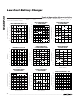
Typical Operating Characteristics (Circuit of Figure 1, adapter = 19.5V, VBATT = 12V, VICTL = 2.4V, MODE > 1.8V, REFON = INPON = LDO, VRELTH = VREF/2, TA = +25°C, unless otherwise noted.) 0 TYPICAL UNIT -5 MINIMUM -10 3.5 3.0 VIN = 19V VIN = 17V 2.5 2.0 1.5 1.0 0.5 -15 2.6 3.1 3.6 4.1 0.5 1.0 1.5 2.0 2.5 SYSTEM CURRENT (A) VCLS (V) MAXIMUM 5 0 -5 MINIMUM 15 MAXIMUM ERROR 10 0 TYPICAL UNIT -5 -10 MINIMUM ERROR 1 0.6 1.2 1.8 2.4 VICTL (V) 3.0 0 -5 -10 -15 4 5 VICTL = 2V 1.3 1.0 0.
Low-Cost Battery Charger SWITCHING FREQUENCY vs. BATTERY VOLTAGE OUTPUT RIPPLE VOLTAGE vs. BATTERY VOLTAGE SWITCHING FREQUENCY (kHz) 0.15 0.12 0.09 0.06 MAX8730 toc11 1000 MAX8730 toc10 OUTPUT RIPPLE VOLTAGE (mVP-P) 0.18 800 600 400 0.03 200 0 0 5 10 15 BATTERY VOLTAGE (V) 0 20 BATTERY REMOVAL 3 6 9 12 BATTERY VOLTAGE (V) 15 18 ADAPTER INSERTION MAX8730toc12 MAX8730toc13 CHARGE CURRENT = 12V 20V ADAPTER COUT = 4.7µF ADAPTER INSERTION 13V 0V 20V PDS 0V 12.
Typical Operating Characteristics (continued) (Circuit of Figure 1, adapter = 19.5V, VBATT = 12V, VICTL = 2.4V, MODE > 1.8V, REFON = INPON = LDO, VRELTH = VREF/2, TA = +25°C, unless otherwise noted.) PEAK-TO-PEAK INDUCTOR CURRENT vs. BATTERY VOLTAGE EFFICIENCY vs. CHARGE CURRENT 2.3 2.1 MAX8730 toc17 100 MAX7830 toc16 90 1.9 EFFICIENCY (%) 1.7 1.5 1.3 3 CELLS 80 1.1 70 0.9 0.7 0.5 3 6 9 12 BATTERY VOLTAGE (V) 15 60 18 0 2.5 2.0 REFON = 1 INPON = 1 1.5 1.0 0.5 3.5 4.
Low-Cost Battery Charger REFERENCE LOAD REGULATION LDO LINE REGULATION -0.360 CHARGER DISABLED -0.13 -0.15 -0.370 -0.17 REF (%) -0.365 -0.375 -0.380 -0.385 -0.19 -0.21 -0.390 -0.23 -0.395 -0.25 -0.400 8 13 18 23 INPUT VOLTAGE (V) 0 28 REF ERROR vs. TEMPERATURE 100 200 300 IREF (µA) 400 500 SWREF LOAD REGULATION -0.05 -0.3 SWREF ERROR (%) -0.10 -0.15 -0.20 MAX8730 toc25 0 MAX8730 toc24 0 REF ERROR (%) MAX8730 toc23 -0.355 LDO ERROR (%) -0.11 MAX8730 toc22 -0.350 -0.
Low-Cost Battery Charger MAX8730 Pin Description PIN NAME FUNCTION 1 ASNS Adapter Voltage Sense. When VASNS > VBATT - 280mV, the battery switch is turned off and the adapter switch is turned on. Connect to the adapter input using an RC filter as shown in Figure 1. 2 LDO Linear-Regulator Output. LDO is the output of the 5.35V linear regulator supplied from SRC. Bypass LDO with a 1µF ceramic capacitor from LDO to GND. 3 SWREF 3.3V Switched Reference.
Low-Cost Battery Charger P2 RS1 15mΩ R3 3kΩ CSSN DHIV PDL R6 6kΩ R5 18kΩ PDS P4 D1 ASNS C4 0.1µF P3 DHI SRC C3 1µF CIN1 4.7µF C12 0.1µF CSSP R1 SYSTEM LOAD C2 10nF C1 32nF MAX8730 P1 ADAPTER INPUT L1 3.5µH R4 75kΩ MAX8730 ACIN REF RS2 30mΩ CSIP R2 CSIN R7 37.4kΩ R9 10kΩ R8 50kΩ BATT REF INPUT ACOK MODE SWREF REF INPUT C5 1µF HOST LDO REF REFON OUTPUT INPON A/D INPUT R13 50kΩ VCTL CLS OUTPUT C6 0.1µF C11 1µF RELTH R12 50kΩ LDO C10 1µF IINP R10 15kΩ COUT2 4.
MAX8730 Low-Cost Battery Charger Detailed Description The MAX8730 includes all the functions necessary to charge Li+, NiMH, and NiCd batteries. A high-efficiency, step-down, DC-DC converter is used to implement a precision constant-current, constant-voltage charger. The DC-DC converter drives a p-channel MOSFET and uses an external free-wheeling Schottky diode.
Low-Cost Battery Charger ASNS PDS MAX8730 RELTH IINP PDL BATT CSSP CSSN SRC CURRENT-SENSE AMPLIFIER CSSP SYSTEM OVERCURRENT GM = 2.8µA/mV A = 20V/V PDS PDL LOGIC REF INPON SRC - 10V SRC REL_EN CCS GND VCTL + 40mV HIGHSIDE DRIVER SRC DHI OVP GMS CLS CCV BATT MODE 222mA CELLSELECT LOGIC GMV LOWEST VOLTAGE CLAMP SELECTOR (DEFAULT = 4.2V) VCTL -5V REGULATOR IMIN DC-DC CONVERTER LVC SRC CCMP REF CCI CHARGER BIAS LOGIC CSIP IMAX CSIN ICTL A = 15V/V CSI LDO REFERENCE 4.
MAX8730 Low-Cost Battery Charger The MAX8730 includes a foldback feature, which reduces the Schottky requirement at low battery voltages. See the Foldback Current Section. Setting Input-Current Limit The total input current, from a wall adapter or other DC source, is the sum of the system supply current and the current required by the charger. When the input current exceeds the set input current limit, the MAX8730 decreases the charge current to provide priority to system load current.
Low-Cost Battery Charger LDO Regulator, REF, and SWREF An integrated linear regulator (LDO) provides a 5.35V supply derived from SRC, and delivers over 10mA of load current. LDO biases the 4.2V reference (REF) and most of the control circuitry. Bypass LDO to GND with a 1µF ceramic capacitor. An additional standalone 1%, 3.3V linear regulator (SWREF) provides 20mA and can remain on when the adapter is absent. Set REFON low to disable SWREF. Set REFON high for normal operation.
MAX8730 Low-Cost Battery Charger CCV, CCI, CCS, and LVC Control Blocks The MAX8730 controls input current (CCS control loop), charge current (CCI control loop), or charge voltage (CCV control loop), depending on the operating condition. The three control loops—CCV, CCI, and CCS—are brought together internally at the lowest voltage clamp (LVC) amplifier. The output of the LVC amplifier is the feedback control signal for the DC-DC controller.
Low-Cost Battery Charger GMOUT = RL (1 + sCOUT × RL) 1 ACSI × RS2 where ACSI = 15V/V and RS2 = 30mΩ in the typical application circuits, so GMOUT = 2.22A/V.
where: VBATT = 16.8V GMV = 0.125µA/mV GMOUT = 2.22A/V COUT = 10µF The loop transfer function is given by: LTF = GMOUT × ACSI × RS × GMI ROGMI 1 + sROGMI × CCI that describes a single-pole system. Since: f OSC = 350kHz (minimum occurs at V IN = 19V and VBATT = 16.8V) RL = 0.
Low-Cost Battery Charger For stability, choose a crossover frequency lower than 1/10 of the switching frequency: CCS = 5 x VIN _ MAX GMS x 2πfOSC VBATT _ MIN Values for CCS greater than 10 times the minimum value may slow down the current-loop response excessively. Figure 9 shows the Bode plot of the input current-limit-loop frequency response using the values calculated above.
MAX8730 Low-Cost Battery Charger MOSFET Drivers The DHI output is optimized for driving moderate-sized power MOSFETs. This is consistent with the variable duty factor that occurs in the notebook computer environment where the battery voltage changes over a wide range. DHI swings from SRC to DHIV and has a typical impedance of 1Ω sourcing and 4Ω sinking. Design Procedure MOSFET Selection Choose the p-channel MOSFETs according to the maximum required charge current.
Low-Cost Battery Charger The ripple current is determined by: The Schottky size and cost can be reduced by utilizing the MAX8730 foldback function. See the Trickle Charge section for more information. The ripple current is only dependent on inductance value and is independent of input and output voltage. See the Ripple Current vs. VBATT graph in the Typical Operating Characteristics. Select the Schottky diode to minimize the battery leakage current when the charger is shut down.
MAX8730 Low-Cost Battery Charger Output Capacitor Selection The output capacitor absorbs the inductor ripple current and must tolerate the surge current delivered from the battery when it is initially plugged into the charger. As such, both capacitance and ESR are important parameters in specifying the output capacitor as a filter and to ensure stability of the DC-DC converter (see the Compensation section).
Low-Cost Battery Charger R7 R14 ICTL R8 Figure 12. ICTL Foldback Current Adjustment For typical applications, choose t Delay = 20µs (depends on the p-MOSFET selected for the PDS switch). The following components can be used for a 10A system short-current design: R10 = 8.66kΩ C6 = 0.1µF R15 = 7.15kΩ C13 = 2.7nF Foldback Current At low duty cycles, most of the charge current is conducted through the Schottky diode (D1).
Pin Configuration GND CCS CCV CCI 21 CSIN TOP VIEW BATT TRANSISTOR COUNT: 3307 PROCESS: BiCMOS CSIP Chip Information 20 19 18 17 16 15 DHIV 22 14 INPON DHI 23 13 REFON SRC 24 12 ICTL CSSN 25 11 IINP 10 MODE MAX8730 CSSP 26 *EXPOSED PADDLE PDS 27 LDO SWREF 4 5 6 7 VCTL 3 ACIN 2 REF 1 CLS + PDL 28 ASNS MAX8730 Low-Cost Battery Charger 5mm x 5mm THIN QFN 28 ______________________________________________________________________________________ 9 ACOK 8 RE
Low-Cost Battery Charger QFN THIN.EPS D2 D MARKING b CL 0.10 M C A B D2/2 D/2 k L AAAAA E/2 E2/2 CL (NE-1) X e E DETAIL A PIN # 1 I.D. E2 PIN # 1 I.D. 0.35x45° e/2 e (ND-1) X e DETAIL B e L L1 CL CL L L e e 0.10 C A C 0.08 C A1 A3 PACKAGE OUTLINE, 16, 20, 28, 32, 40L THIN QFN, 5x5x0.8mm -DRAWING NOT TO SCALE- COMMON DIMENSIONS A1 A3 b D E e 0.70 0.75 0.80 0.70 0.75 0.80 0.70 0.75 0.80 0.70 0.75 0.80 0.70 0.75 0.80 0 0.02 0.05 0 0.02 0.05 0 0.02 0.