
User guide


MAX8737
provide good transient response, the capacitor’s ESR
should be minimized:
∆V
OUT
= ∆I
OUT
x ESR
where ∆I
OUT
is the maximum peak-to-peak load current
step, and ∆V
OUT
is the transient output-voltage tolerance.
Regulator Compensation
The compensation network (R3_, C2_) is customizable
and depends on load and MOSFET characteristics:
• Use of ceramic output capacitors with low R
ESR
to
ensure stability and minimize ESR voltage drop at
load step
•Strength of the external n-channel MOSFET (g
M
), its
forward transconductance (g
FS
), and the gate-to-
source capacitance (C
GS
)
• The driver transconductance (G
MDRV
) of the inte-
grated circuit driver
• Load current range (including the minimum load):
I
MIN
to I
MAX
Recommended Procedure
Use the C
GS
,g
FS,
I
D
from the chosen transistor data
sheet and use the equation below to translate the mea-
sured g
FS
to g
M
for normal operation:
1) Determine the LDO transconductance using the
MOSFET’s forward transconductance (g
FS
), and the
drain current (I
D
) used to test the selected MOSFET:
2) Calculate the compensation resistor based on the
output capacitor (C
OUT
), the MOSFET’s gate-to-
source capacitance (C
GS
= C
ISS
- C
RSS
), and the
minimum driver transconductance:
3) Calculate the compensation capacitance using the
minimum load current (I
MIN
) and compensation
resistor value calculated above:
where V
T
= 25mV.
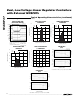
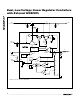
Example: The example below is used to demonstrate
the stability calculation for the application circuit in
Figure 1.
1) Choose V
OUT
= 1.05V and I
MAX
= 3A and the mini-
mum load can be determined from the foldback cur-
rent-limit resistance:
2) For the selected MOSFET (Si4922DY), C
GS
=
2000pF at 1.5V, and g
FS
= 30S at I
D
= 8.8A:
3) The output capacitor must be at least 4.7µF/A.
Therefore the design must use a minimum 14.1µF
capacitor. The closest standard capacitor value is
22µF.
4) Based on the above operating conditions and com-
ponent selection, the compensation resistor value
should be:
5) Finally, select the compensation capacitor value:
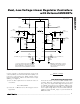
External MOSFET Selection
The MAX8737 uses an n-channel MOSFET as the
series pass transistor instead of a p-channel MOSFET
to reduce cost. The selected MOSFET must have a
gate threshold voltage (at the required max load) that
meets the following criteria:
where V
CC
is the controller bias voltage, and V
GS_MAX
is the maximum gate voltage required to yield the on-
resistance (R
DS_ON
) specified by the manufacturer’s
data sheet. Make sure that input-to-output voltage
meets the condition below to avoid entering dropout,
where output voltage starts to decrease and any ripple
on the input also passes through to the output. R
DSON
has a positive temperature coefficient (approximately
VVV
GS MAX CC OUT_
≤−
C
mV F
mA S
F2
225 22
6135
015
2
=
××
××
=
µ
µ
()
.
Ω
R
F
nF S S
3
22
217505
35=
××
=
µ
..
Ω
gS
A
A
S
M
==30
3
88
17 5
.
.
I
V
RR
mA
MIN
OUT
=
+
≈
12
6
C
VC
IG R
T OUT
MIN MDRV
2
2
3
2
=
()
R
C
Cgx S
OUT
GS M
3
05
=
.
gg
I
I
MFS
MAX
D
=
Dual, Low-Voltage Linear Regulator Controllers
with External MOSFETs
12 ______________________________________________________________________________________