
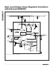
User guide


0.5%/°C); therefore, the value of R
DSON
at the highest
operating junction temperature should be used:
where V
IN_MIN
is the minimum input voltage at the drain
of the MOSFET.
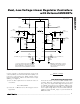
MOSFET Power Dissipation
The maximum power dissipation of the MAX8737
depends on the thermal resistance of the external n-
channel MOSFET package, the board layout, the tem-
perature difference between the die and ambient air,
and the rate of airflow. The power dissipated in the
MOSFET is:
P
DIS
= I
OUT
(V
IN
- V
CSP
)
The maximum allowable power dissipation is deter-
mined by the following formula:
where T
J(MAX)
is the maximum junction temperature
(+150°C), T
A
is the ambient temperature, θ
JC
is the
thermal resistance from the die junction to the package
case, and θ
CA
is the thermal resistance from the case
through the PC board, copper traces, and other materi-
als to the surrounding air. Standard 8-pin SO MOSFETs
are typically rated for 2W, while new power packages
(PowerPAK™, DirectFET™, etc.) can achieve power
dissipation ratings as high as 5W. For optimum power
dissipation, use a large ground plane with good ther-
mal contact to ground and use wide input and output
traces. Extra copper on the PC board increases ther-
mal mass and reduces the thermal resistance of the
board. See Figure 4.
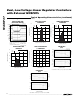
PC Board Layout Guidelines
Due to the high-current paths and tight output accuracy
required by most applications, careful PC board layout
is required. An evaluation kit (MAX8737EVKIT) is avail-
able to speed design. It is important to keep all
traces as short as possible to minimize the high-
current trace dimensions to reduce the effect of
undesirable parasitic inductance. The MOSFET dissi-
pates a fair amount of heat due to the high currents
involved, especially during large input-to-output voltage
differences. To dissipate the heat generated by the
MOSFET, make power traces very wide with a large
amount of copper area. An efficient way to achieve
good power dissipation on a surface-mount package is
to lay out copper areas directly under the MOSFET
package on multiple layers and connect the areas
through vias. Use a ground plane to minimize imped-
ance and inductance.
In addition to the usual high-power considerations, here
are four tips to ensure high output accuracy:
• Ensure that the feedback connection to C
OUT
is
short and direct.
• Place the reference input resistors next to the
REFIN_ pin.
• Place RC and CC next to the DRV_ pin.
• Ensure REFIN_ and DRV_ traces are away from
noisy sources to ensure tight accuracy.
R
TT
DIS MAX
J MAX A
JC CA
()
()
=
−
+θθ
VV IR R
IN MIN OUT MAX MAX DSON MAX CS__ _
()−≥ +
MAX8737
Dual, Low-Voltage Linear Regulator Controllers
with External MOSFETs
______________________________________________________________________________________ 13
PowerPAK is a registered trademark of Vishay Siliconix.
DirectFET is a trademark of International Rectifier Corp.