
User guide

MAX8737
Dual, Low-Voltage Linear Regulator Controllers
with External MOSFETs
2 _______________________________________________________________________________________
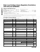
ABSOLUTE MAXIMUM RATINGS
Stresses beyond those listed under “Absolute Maximum Ratings” may cause permanent damage to the device. These are stress ratings only, and functional
operation of the device at these or any other conditions beyond those indicated in the operational sections of the specifications is not implied. Exposure to
absolute maximum rating conditions for extended periods may affect device reliability.
V
CC
to GND..............................................................-0.3V to +6V
OUT1, OUT2 to GND................................................-0.3V to +6V
REFIN1, REFIN2, PGOOD1, PGOOD2, EN1,
EN2 to GND..........................................................-0.3V to +6V
DRV1, DRV2, CS1, CS2 to GND.................-0.3V to (V
CC
+ 0.3V)
Continuous Power Dissipation (T
A
= +70°C)
16-Pin 4mm x 4mm Thin QFN (derated 25mW/°C
above +70°C).............................................................2000mW
Operating Temperature Range
MAX8737ETE...................................................-40°C to +85°C
Junction Temperature......................................................+150°C
Storage Temperature Range .............................-65°C to +150°C
Lead Temperature (soldering, 10s) .................................+300°C
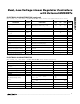
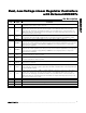
ELECTRICAL CHARACTERISTICS
(V
CC
= 5V, EN_ = CS_ = V
CC
, V
REFIN
= 1.0V, T
A
= 0°C to +85°C, unless otherwise noted. Typical values are at T
A
= +25°C.)
PARAMETER
SYMBOL
CONDITIONS
MIN TYP MAX
UNITS
Supply Voltage Range V
CC
4.75 5.50
V
V
CC
Undervoltage Lockout
Threshold
Rising edge, 200mV hysteresis (typ) 4.1
4.35
4.6 V
V
CC
Quiescent Supply Current I
CC
EN1 = EN2 = V
CC
0.5 1 mA
V
CC
Shutdown Supply Current EN1 = EN2 = GND 0.1 5 µA
REFIN to OUT Offset Voltage V
OUT
_-5+5mV
OUT_ Input Bias Current I
OUT
_-1+1µA
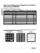
DRIVERS
Output high; V
OUT
_ = V
REFIN
_ - 25mV,
I
LOAD
= 1mA
V
CC
-
0.3
V
CC
-
0.05
DRV_ Output Voltage Swing
(Note 1)
Output low; V
OUT
_ = V
REFIN
_ + 25mV,
I
LOAD
= 1mA
0.03
0.3
V
DRV_ Maximum Sourcing Current
V
OUT
_ = V
REFIN
_ - 25mV; V
DRV
= 3V 6 14 mA
DRV_ Maximum Sinking Current V
OUT
_ = V
REFIN
_ + 25mV; V
DRV
= 3V 6 14 mA
OUT_ to DRV_ Transconductance
(Large Signal)
G
MDRV
0.8 S
DRV_ Power-Supply Rejection
Ratio
10Hz < f < 10kHz, I
DRV
= 1mA, C
DRV
=
10nF
-80 dB
DRV_ Soft-Start Charging Current
I
SOFT
40 170
400
µA
REFERENCE INPUT
REFIN_ Voltage Range
V
REFIN
_
V
CC
= 4.75V to 5.5V 0.5 2.5 V
REFIN_ Input Bias Current I
REFIN
_V
REFIN
_ = 0 to 2.5V
-100
-10
+100
nA
FAULT PROTECTION
Thermal Shutdown Threshold T
SHDN
Hysteresis = 20°C
+125
°C
T
A
= 0°C to +85°C 7 10 13
Current-Limit Threshold V
ILIM
V
CS
_ - V
OUT
_
T
A
= +85°C 7.5 10
12.5
mV
CS_ Input Current -1 +1 µA
Linear Regulator UVP Threshold
(Slow)
UVP
(
SLOW
)
With respect to V
REFIN
; CS_ = V
CC
72 80 88 %