
User guide
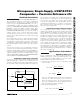

MAX9039–MAX9043/MAX9050–MAX9053
Micropower, Single-Supply, UCSP/SOT23
Comparator + Precision Reference ICs
2 _______________________________________________________________________________________
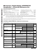
ABSOLUTE MAXIMUM RATINGS
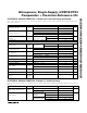
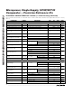
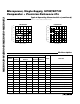
ELECTRICAL CHARACTERISTICS—A Grade (0.4% Initial Accuracy)
(V
CC
= +5V, V
EE
= 0V, V
CM
= 0V, I
OUT
= 0A, I
REF
= 0A, T
A
= T
MIN
to T
MAX
, unless otherwise noted. Typical values are at
T
A
= +25°C.) (Note 2)
Stresses beyond those listed under “Absolute Maximum Ratings” may cause permanent damage to the device. These are stress ratings only, and functional
operation of the device at these or any other conditions beyond those indicated in the operational sections of the specifications is not implied. Exposure to
absolute maximum rating conditions for extended periods may affect device reliability.
Supply Voltage (V
CC
to V
EE
) ....................................-0.3V to +6V
All Other Pins ...................................(V
EE
- 0.3V) to (V
CC
+ 0.3V)
Output Short-Circuit Duration
(OUT_, REF) ...............Indefinite Short Circuit to Either Supply
Continuous Power Dissipation (T
A
= +70°C)
5-Pin SOT23 (derate 7.10mW/°C above +70°C)..........571mW
6-Bump UCSP (derate 3.9mW/°C above +70°C) ........308mW
6-Pin SOT23 (derate 8.70mW/°C above +70°C)..........696mW
8-Pin SO (derate 5.88mW/°C above +70°C)................471mW
8-Pin µMAX (derate 4.1mW/°C above +70°C) .............330mW
10-Pin µMAX (derate 5.6mW/°C above +70°C) ...........444mW
Operating Temperature Range ...........................-40°C to +85°C
Junction Temperature......................................................+150°C
Storage Temperature Range .............................-65°C to +150°C
Lead Temperature (soldering, 10s) .................................+300°C
Bump Reflow Temperature (Note 1) ................................+235°C
Note 1: This device is constructed using a unique set of packaging techniques that impose a limit on the thermal profile the device
can be exposed to during board-level solder attach and rework. This limit permits only the use of the solder profiles recom-
mended in the industry-standard specification, JEDEC 020A, paragraph 7.6, Table 3 for IR/VPR and Convection Packaging
Reflow. Preheating is required. Hand or wave soldering is not allowed.
PARAMETER SYMBOL CONDITIONS MIN TYP MAX UNITS
MAX9040–MAX9043 2.5 5.5
Supply Voltage Range (Note 3) V
CC
MAX9050–MAX9053 2.7 5.5
V
V
CC
= 2.7V 47 67
MAX9040/MAX9041/
MAX9050/MAX9051
V
CC
= 5V 52 72
V
CC
= 2.7V 55 80
Supply Current I
CC
MAX9042/MAX9043/
MAX9052/MAX9053
V
CC
= 5V 60 85
µA
COMPARATORS
T
A
= +25°C ±0.5 ±5.0
Input Offset Voltage (Note 4) V
OS
Over entire
common-mode
range
T
A
= -40°C to +85°C ±7.0
mV
Input Hysteresis V
HYST
±3.0 mV
Input Bias Current
(Notes 5, 6, 7)
I
B
Specified common-mode range ±0.001 ±10.0 nA
Input Offset Current (Note 5) I
OS
Specified common-mode range ±0.5 pA
T
A
= +25°C
V
EE
-
0.25
V
CC
+
0.25
Common-Mode Voltage Range
(Notes 5, 8)
CMVR
T
A
= -40°C to +85°CV
EE
V
CC
V
Common-Mode Rejection Ratio
(Note 5)
CMRR Specified common-mode range 52 80 dB
MAX9040–MAX9043, 2.5V ≤ V
CC
≤ 5.5V 55 80
Power-Supply Rejection Ratio PSRR
MAX9050–MAX9053, 2.5V ≤ V
CC
≤ 5.5V 55 80
dB
Input Capacitance (Note 5) C
IN
2.5 pF
V
CC
= 5V 95
Output Short-Circuit Current I
SC
V
OUT
=
V
EE
or V
CC
V
CC
= 2.7V 35
mA
V
CC
= 5V, I
SINK
= 8mA 0.2 0.55
Output Voltage Low V
OL
V
CC
= 2.7V, I
SINK
= 3.5mA 0.15 0.4
V